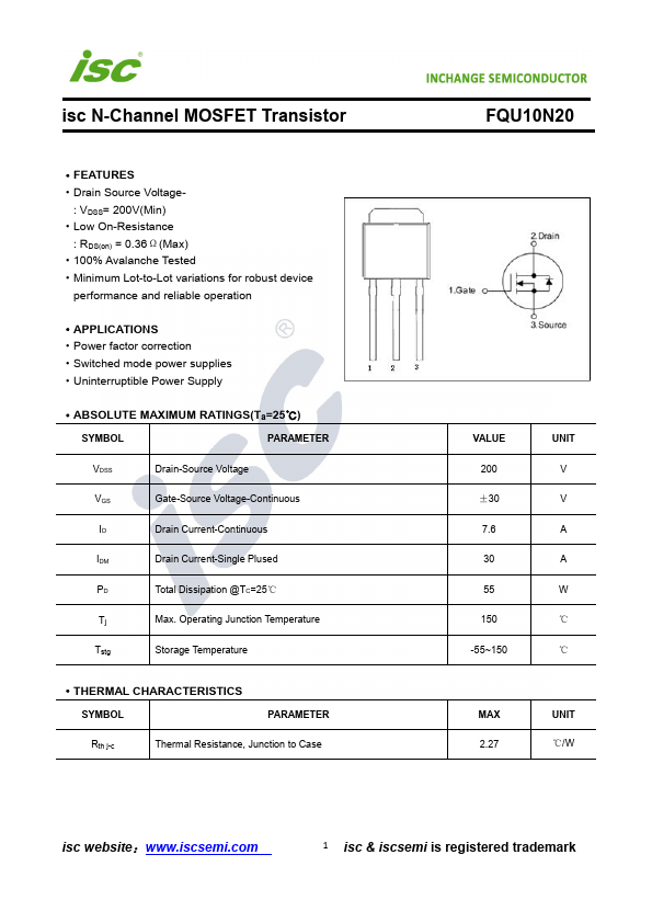
FQU10N20
FEATURES
- Drain Source Voltage-
: VDSS= 200V(Min)
- Low On-Resistance
: RDS(on) = 0.36Ω(Max)
- 100% Avalanche Tested
- Minimum Lot-to-Lot variations for robust device performance and reliable operation
- APPLICATIONS
- Power factor correction
- Switched mode power supplies
- Uninterruptible Power Supply
- ABSOLUTE MAXIMUM RATINGS(Ta=25℃)
SYMBOL
PARAMETER
VDSS
Drain-Source Voltage
Gate-Source Voltage-Continuous
Drain Current-Continuous
Drain Current-Single Plused
Total Dissipation @TC=25℃
Tj
Max. Operating Junction Temperature
Tstg
Storage Temperature
- THERMAL CHARACTERISTICS
SYMBOL
PARAMETER
Rth j-c
Thermal Resistance, Junction to Case
VALUE 200 ±30 7.6 30 55 150
-55~150
UNIT V V A A W ℃ ℃
MAX 2.27
UNIT ℃/W isc website:.iscsemi.
1 isc & iscsemi is registered trademark isc N-Channel MOSFET Transistor
- ELECTRICAL CHARACTERISTICS...