Full PDF Text Transcription for FQA140N10 (Reference)
Note: Below is a high-fidelity text extraction (approx. 800 characters) for
FQA140N10. For precise diagrams, and layout, please refer to the original PDF.
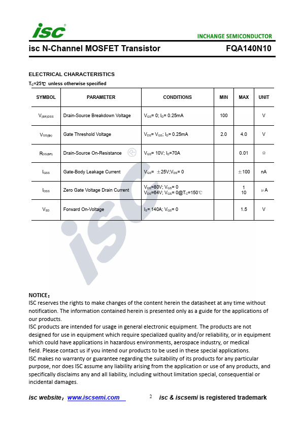
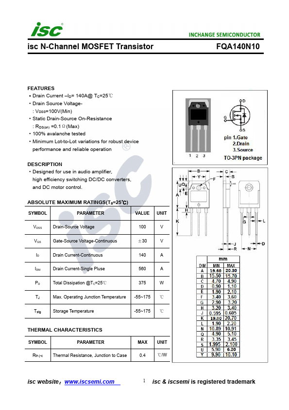
ltage- : VDSS=100V(Min) ·Static Drain-Source On-Resistance : RDS(on) =0.1Ω(Max) ·100% avalanche tested ·Minimum Lot-to-Lot variations for robust device performance and reliable operation DESCRIPTION ·Designed for use in audio amplifier, high efficiency switching DC/DC converters, and DC motor control. ABSOLUTE MAXIMUM RATINGS(Ta=25℃) SYMBOL PARAMETER VALUE UNIT VDSS Drain-Source Voltage 100 V VGS Gate-Source Voltage-Continuous ±30 V ID Drain Current-Continuous 140 A IDM Drain Current-Single Pluse 560 A PD Total Dissipation @TC=25℃ 375 W TJ Max.
 FQA140N10 Datasheet