Click to expand full text
isc Silicon NPN Power Transistor
INCHANGE Semiconductor
BDW12
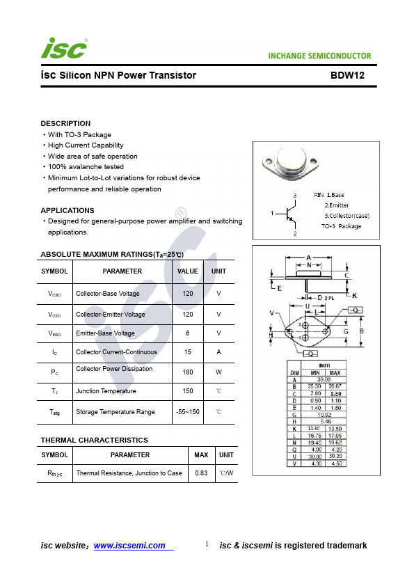
DESCRIPTION ·With TO-3 Package ·High Current Capability ·Wide area of safe operation ·100% avalanche tested ·Minimum Lot-to-Lot variations for robust device
performance and reliable operation
APPLICATIONS ·Designed for general-purpose power amplifier and switching
applications.
ABSOLUTE MAXIMUM RATINGS(Ta=25℃)
SYMBOL
PARAMETER
VALUE
UNIT
VCBO
Collector-Base Voltage
VCEO VEBO
IC PC TJ
Collector-Emitter Voltage Emitter-Base Voltage Collector Current-Continuous Collector Power Dissipation
Junction Temperature
Tstg
Storage Temperature Range
120
V
120
V
6
V
15
A
180
W
150
℃
-55~150
℃
THERMAL CHARACTERISTICS
SYMBOL
PARAMETER
MAX UNIT
Rth j-c Thermal Resistance, Junction to Case 0.
 BDW12 Datasheet