Click to expand full text
TECHNICAL DATA
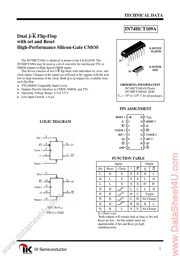
IN74HCT109A Dual J-K Flip-Flop with set and Reset High-Performance Silicon-Gate CMOS
The IN74HCT109A is identical in pinout to the LS/ALS109. The IN74HCT109A may be used as a level converter for interfacing TTL or NMOS outputs to High Speed CMOS inputs. This device consists of two J-K flip-flops with individual set, reset, and clock inputs. Changes at the inputs are reflected at the outputs with the next low-to-high transition of the clock. Both Q to Q outputs are available from each flip-flop. • TTL/NMOS Compatible Input Levels • Outputs Directly Interface to CMOS, NMOS, and TTL • Operating Voltage Range: 4.5 to 5.5 V • Low Input Current: 1.0 µA
ORDERING INFORMATION IN74HCT109AN Plastic IN74HCT109AD SOIC TA = -55° to 125° C for all packages.
 IN74HCT109A Datasheet