Click to expand full text
FemtoClock® NG Crystal-to-LVDS Clock Synthesizer
844N255I
Data Sheet
General Description
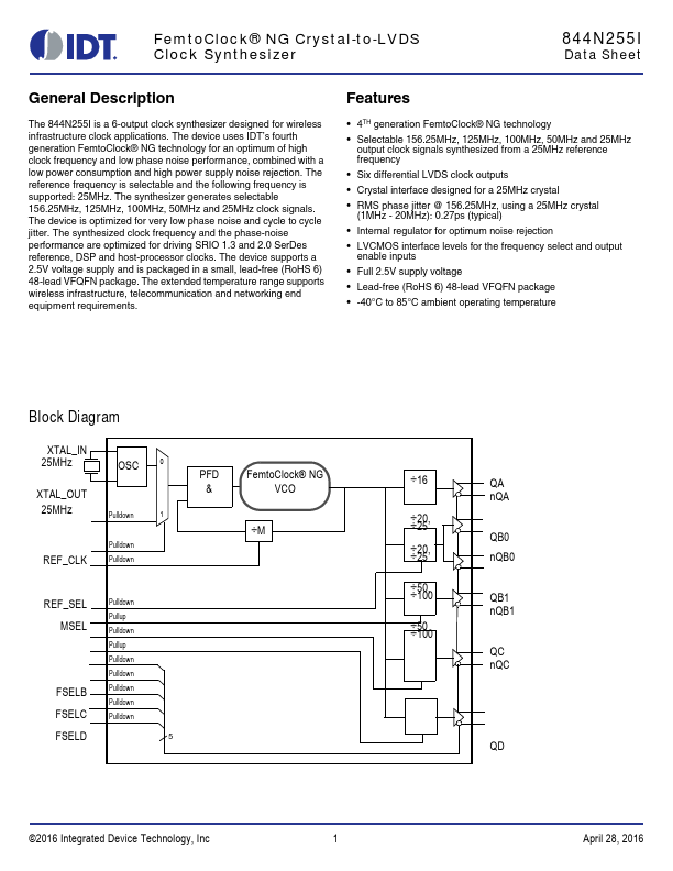
The 844N255I is a 6-output clock synthesizer designed for wireless infrastructure clock applications. The device uses IDT’s fourth generation FemtoClock® NG technology for an optimum of high clock frequency and low phase noise performance, combined with a low power consumption and high power supply noise rejection. The reference frequency is selectable and the following frequency is supported: 25MHz. The synthesizer generates selectable 156.25MHz, 125MHz, 100MHz, 50MHz and 25MHz clock signals. The device is optimized for very low phase noise and cycle to cycle jitter. The synthesized clock frequency and the phase-noise performance are optimized for driving SRIO 1.3 and 2.
 844N255I Datasheet