Datasheet4U Logo Datasheet4U.com

HY5W2A6C - 4 Bank x 2 M x 16 Bit Synchronous DRAM

Description

and is subject to change without notice.

Hynix does not assume any responsibility for use of circuits described.

No patent licenses are implied.

Features

  • Standard SDRAM Protocol Internal 4bank operation Voltage : VDD = 2.5V, VDDQ = 1.8V & 2.5V LVTTL compatible I/O Interface Low Voltage interface to reduce I/O power Low Power Features ( HY5W26CF / HY57W281620HCT series can’t support these features) - PASR(Partial Array Self Refresh) - TCSR(Temperature Compensated Self Refresh) - Deep Power Down Mode CAS latency of 1, 2, or 3 Packages : 54ball, 0.8mm pitch FBGA / 54pin, TSOP -25 ~ 70C Oper.

📥 Download Datasheet

Datasheet Details

Part number HY5W2A6C
Manufacturer SK Hynix
File Size 321.52 KB
Description 4 Bank x 2 M x 16 Bit Synchronous DRAM
Datasheet download datasheet HY5W2A6C Datasheet

Full PDF Text Transcription

Click to expand full text
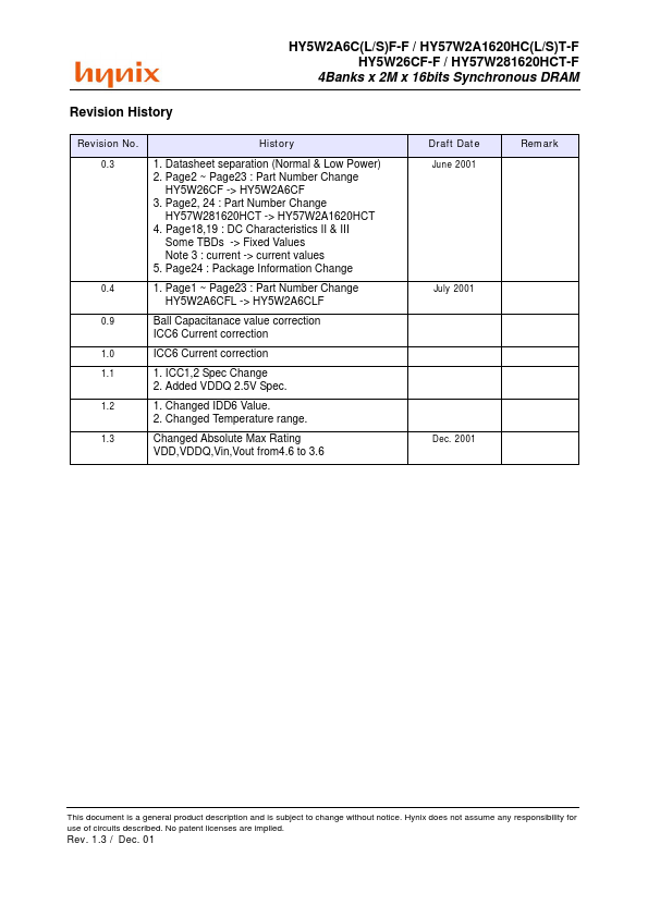
HY5W2A6C(L/S)F-F / HY57W2A1620HC(L/S)T-F HY5W26CF-F / HY57W281620HCT-F 4Banks x 2M x 16bits Synchronous DRAM Revision History Revision No. 0.3 History Draft Date June 2001 Remark 1. Datasheet separation (Normal & Low Power) 2. Page2 ~ Page23 : Part Number Change HY5W26CF -> HY5W2A6CF 3. Page2, 24 : Part Number Change HY57W281620HCT -> HY57W2A1620HCT 4. Page18,19 : DC Characteristics II & III Some TBDs -> Fixed Values Note 3 : current -> current values 5. Page24 : Package Information Change 1. Page1 ~ Page23 : Part Number Change HY5W2A6CFL -> HY5W2A6CLF Ball Capacitanace value correction ICC6 Current correction ICC6 Current correction 1. ICC1,2 Spec Change 2. Added VDDQ 2.5V Spec. 1. Changed IDD6 Value. 2. Changed Temperature range. Changed Absolute Max Rating VDD,VDDQ,Vin,Vout from4.
Published: |