Datasheet Details
| Part number | HYMP125P72CP4L-C4 |
|---|---|
| Manufacturer | SK Hynix |
| File Size | 808.80 KB |
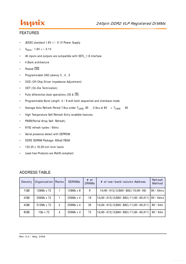
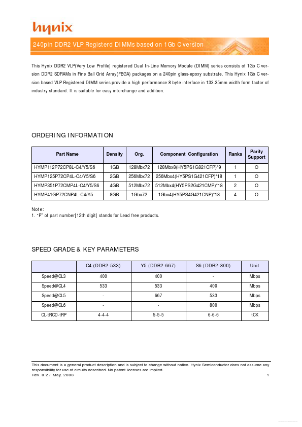
| Description | 240pin DDR2 VLP Registerd DIMMs based on 1Gb C version |
| Datasheet |
 HYMP125P72CP4L-C4 Datasheet HYMP125P72CP4L-C4 Datasheet
|
|
|
Download the HYMP125P72CP4L-C4 datasheet PDF. This datasheet also covers the HYMP112P72CP8L-C4 variant, as both devices belong to the same 240pin ddr2 vlp registerd dimms based on 1gb c version family and are provided as variant models within a single manufacturer datasheet.
and is subject to change without notice.
Hynix Semiconductor does not assume any responsibility for use of circuits described.
No patent licenses are implied.
| Part number | HYMP125P72CP4L-C4 |
|---|---|
| Manufacturer | SK Hynix |
| File Size | 808.80 KB |
| Description | 240pin DDR2 VLP Registerd DIMMs based on 1Gb C version |
| Datasheet |
HYMP125P72CP4L-C4 Datasheet
|
|
|
|
| Part Number | Description | Manufacturer |
|---|---|---|
| HYMP512R72x | 128M x 72 Bits DDR2 SDRAM Registered DIMM | Hynix |
| HYMP512Rxxx | DDR2 SDRAM Unbuffered DIMMs Based on 512M | Hynix |
| HYMP512S64CLP8-C4 | 200pin Unbuffered DDR2 SDRAM SO-DIMMs based on 512 Mb | Hynix |
| HYMP512S64CLP8-E3 | 200pin Unbuffered DDR2 SDRAM SO-DIMMs based on 512 Mb | Hynix |
| HYMP512S64CLP8-S5 | 200pin Unbuffered DDR2 SDRAM SO-DIMMs based on 512 Mb | Hynix |
| Part Number | Description |
|---|---|
| HYMP125P72CP4L-S6 | 240pin DDR2 VLP Registerd DIMMs based on 1Gb C version |
| HYMP125P72CP4L-Y5 | 240pin DDR2 VLP Registerd DIMMs based on 1Gb C version |
| HYMP125P72CP4-C4 | 240pin Registered DDR2 SDRAM DIMMs based on 1Gb |
| HYMP125P72CP4-S5 | 240pin Registered DDR2 SDRAM DIMMs based on 1Gb |
| HYMP125P72CP4-S6 | 240pin Registered DDR2 SDRAM DIMMs based on 1Gb |