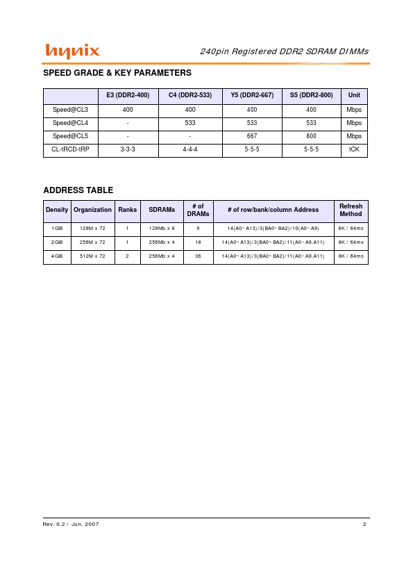
Datasheet4U Logo Datasheet4U.com

HYMP112P72CP8-Y5 - 240pin Registered DDR2 SDRAM DIMMs based on 1Gb

This page provides the datasheet information for the HYMP112P72CP8-Y5, a member of the HYMP112P72CP8-C4 240pin Registered DDR2 SDRAM DIMMs based on 1Gb family.

Description

and is subject to change without notice.

Hynix Semiconductor does not assume any responsibility for use of circuits described.

No patent licenses are implied.

Features

  • JEDEC standard Double Data Rate2 Synchronous DRAMs (DDR2 SDRAMs) with 1.8V +/0.1V Power Supply All inputs and outputs are compatible with SSTL_1.8 interface 8 Bank architecture Posted CAS Programmable CAS Latency 3 , 4 , 5 OCD (Off-Chip Driver Impedance Adjustment) ODT (On-Die Termination).
  • Fully differential clock operations (CK & CK) Programmable Burst Length 4 / 8 with both sequential and interleave mode.

📥 Download Datasheet

Datasheet preview – HYMP112P72CP8-Y5

Datasheet Details

Part number HYMP112P72CP8-Y5
Manufacturer Hynix Semiconductor
File Size 256.88 KB
Description 240pin Registered DDR2 SDRAM DIMMs based on 1Gb
Datasheet download datasheet HYMP112P72CP8-Y5 Datasheet
Additional preview pages of the HYMP112P72CP8-Y5 datasheet.
Other Datasheets by Hynix Semiconductor

Full PDF Text Transcription

Click to expand full text
240pin Registered DDR2 SDRAM DIMMs based on 1Gb version C This Hynix Registered Dual In-Line Memory Module (DIMM) series consists of 1Gb version C DDR2 SDRAMs in Fine Ball Grid Array(FBGA) packages on a 240pin glass-epoxy substrate. This Hynix 1Gb version C based Registered DDR2 DIMM series provide a high performance 8 byte interface in 5.25" width form factor of industry standard. It is suitable for easy interchange and addition. FEATURES • JEDEC standard Double Data Rate2 Synchronous DRAMs (DDR2 SDRAMs) with 1.8V +/0.1V Power Supply All inputs and outputs are compatible with SSTL_1.
Published: |