Click to expand full text
www.DataSheet4U.com
HY5DV281622DT
128M(8Mx16) GDDR SDRAM
HY5DV281622DT
This document is a general product description and is subject to change without notice. Hynix Electronics does not assume any responsibility for use of circuits described. No patent licenses are implied. Rev. 0.5 / Aug. 2003
HY5DV281622DT
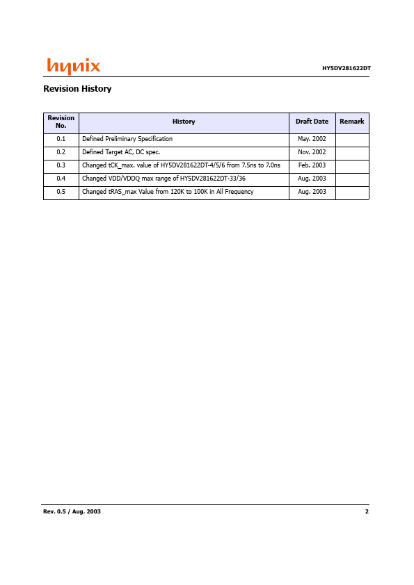
Revision History
Revision No. 0.1 0.2 0.3 0.4 0.5
History Defined Preliminary Specification Defined Target AC, DC spec. Changed tCK_max. value of HY5DV281622DT-4/5/6 from 7.5ns to 7.0ns Changed VDD/VDDQ max range of HY5DV281622DT-33/36 Changed tRAS_max Value from 120K to 100K in All Frequency
Draft Date May. 2002 Nov. 2002 Feb. 2003 Aug. 2003 Aug. 2003
Remark
Rev. 0.5 / Aug.
 HY5DV281622DT Datasheet