Click to expand full text
( DataSheet : www.DataSheet4U.com )
0.1 : Hynix Change 0.2 : 143Mhz Add, Burst read single write mode correction
www.DataSheet4U.com
www.DataSheet4U.com
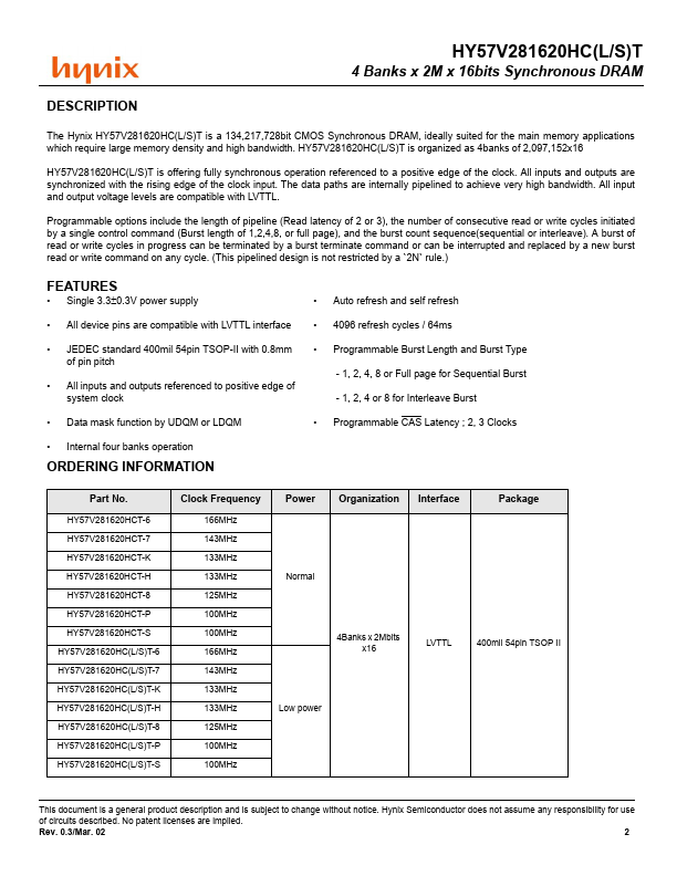
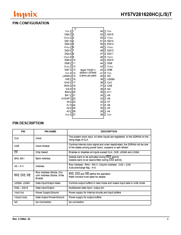
HY57V281620HC(L/S)T
4 Banks x 2M x 16bits Synchronous DRAM
DESCRIPTION
The Hynix HY57V281620HC(L/S)T is a 134,217,728bit CMOS Synchronous DRAM, ideally suited for the main memory applications which require large memory density and high bandwidth. HY57V281620HC(L/S)T is organized as 4banks of 2,097,152x16 HY57V281620HC(L/S)T is offering fully synchronous operation referenced to a positive edge of the clock. All inputs and outputs are synchronized with the rising edge of the clock input. The data paths are internally pipelined to achieve very high bandwidth. All input and output voltage levels are compatible with LVTTL.
 HY57V281620HCT Datasheet