Click to expand full text
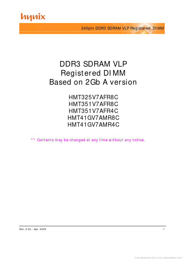
240pin DDR3 SDRAM VLP Registered DIMM
DDR3 SDRAM VLP Registered DIMM Based on 2Gb A version
HMT325V7AFR8C HMT351V7AFR8C HMT351V7AFR4C HMT41GV7AMR8C HMT41GV7AMR4C
** Contents may be changed at any time without any notice.
Rev. 0.02 / Apr. 2009
1
Free Datasheet http://www.datasheet4u.com/
Revision History
Revision No. 0.01 0.02 History Initial Release Added IDD Specificaion Draft Date 2009-04 2009-04 Remark
Rev. 0.02 / Apr. 2009
2
Free Datasheet http://www.datasheet4u.com/
Table of Contents
1. Description 1.1 Device Features and Ordering Information 1.1.1 Features 1.1.2 Ordering Information 1.2 Speed Grade & Key Parameters 1.3 Address Table 2. Pin Architecture 2.1 Pin Definition 2.2 Input/Output Functional Description 2.3 Pin Assignment 3. Functional Block Diagram 3.
 HMT41GV7AMR4C Datasheet