Click to expand full text
HT9926
N-Channel Enhancement Mode Field Effect Transistor
FEATURES
Super high dense cell design for low RDS(ON)。
Rugged and reliable. SOP-8 package. Pb Free.
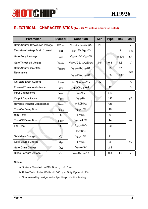
VDS (V) 20V
Product Summary
ID (A) 6A
RDS(ON) (mΩ) Max 32 @VGS = 4.0V 43 @VGS = 2.5V
SOP-8 ABSOLUTE MAXIMUM RATINGS (TA = 25 0C unless otherwise noted)
Parameter
Drain-Source Voltage
Gate-Source Voltage Drain Current-Continuous @ TC = 25 C -Pulse db Drain-Source Diode Forward Current a Maximum Power Dissipation a Operating Junction and Storage Temperature Range
THERMAL CHARACTERISTICS
Thermal Resistance, Junction-to-Ambient a Ver1.0
RθJA
Symbol
VDS VGS ID IDM IS PD TJ, TSTG
Limit
20 ±10
6 35 1.7 2 -55 to 150
Unit
V V A A A W 0C
62.
 HT9926 Datasheet