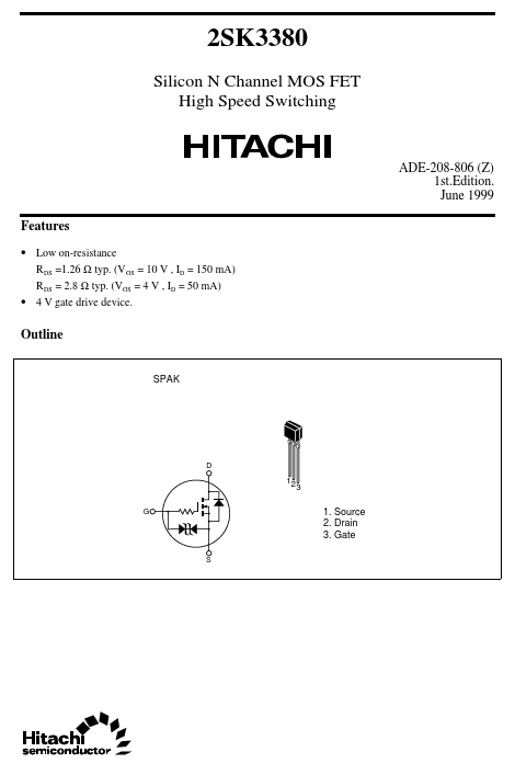
Low on-resistance RDS =1.26 Ω typ. (VGS = 10 V , ID = 150 mA) RDS = 2.8 Ω typ. (VGS = 4 V , ID = 50 mA).
4 V gate drive device. Outline
SPAK
ADE-208-806 (Z) 1st. Edition. June 1999
D G
S
123
1. Source 2. Drain 3. Gate
2SK3380
Absolute Maximum Ratings (Ta = 25°C)
Item
Symbol
Drain to source voltage Gate to source voltage Drain current Drain peak current Body-drain diode reverse drain current Channel dissipation
VDSS VGSS ID I Note1
D(pulse)
I DR Pch
Channel temperature.
Note: Below is a high-fidelity text extraction (approx. 800 characters) for
K3380. For precise diagrams, and layout, please refer to the original PDF.
2SK3380 Silicon N Channel MOS FET High Speed Switching Features • Low on-resistance RDS =1.26 Ω typ. (VGS = 10 V , ID = 150 mA) RDS = 2.8 Ω typ. (VGS = 4 V , ID = 50 mA) ...
View more extracted text
(VGS = 10 V , ID = 150 mA) RDS = 2.8 Ω typ. (VGS = 4 V , ID = 50 mA) • 4 V gate drive device. Outline SPAK ADE-208-806 (Z) 1st.Edition. June 1999 D G S 123 1. Source 2. Drain 3. Gate 2SK3380 Absolute Maximum Ratings (Ta = 25°C) Item Symbol Drain to source voltage Gate to source voltage Drain current Drain peak current Body-drain diode reverse drain current Channel dissipation VDSS VGSS ID I Note1 D(pulse) I DR Pch Channel temperature Tch Storage temperature Tstg Note: 1. PW ≤ 10 µs, duty cycle ≤ 1% Ratings 30 ±20 300 1.
More Datasheets from Hitachi Semiconductor (now Renesas)
 K3380 Datasheet