Click to expand full text
www.DataSheet4U.com
HD74SSTV16857
1:1 14-bit SSTL_2 Registered Buffer
ADE-205-336F (Z) Rev.6 June. 2001 Description
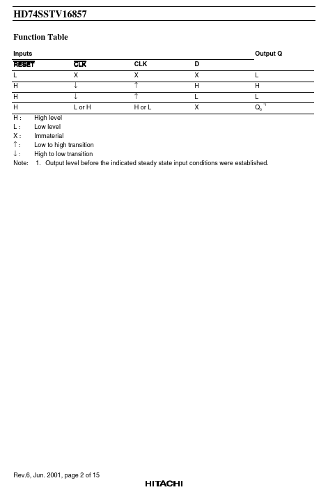
The HD74SSTV16857 is a 14-bit registered buffer designed for 2.3 V to 2.7 V Vcc operation and LVCMOS reset (RESET) input / SSTL_2 data (D) inputs and CLK input. Data flow from D to Q is controlled by differential clock pins (CLK, CLK) and the RESET. Data is triggered on the positive edge of the positive clock (CLK), and the negative clock (CLK) must be used to maintain noise margins. When RESET is low, all registers are reset and all outputs are low. To ensure defined outputs from the register before a stable clock has been supplied, RESET must be held in the low state during power up.
 HD74SSTV16857 Datasheet