Click to expand full text
HD74HC673
16-bit Shift Register
Description
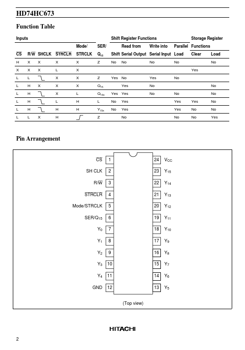
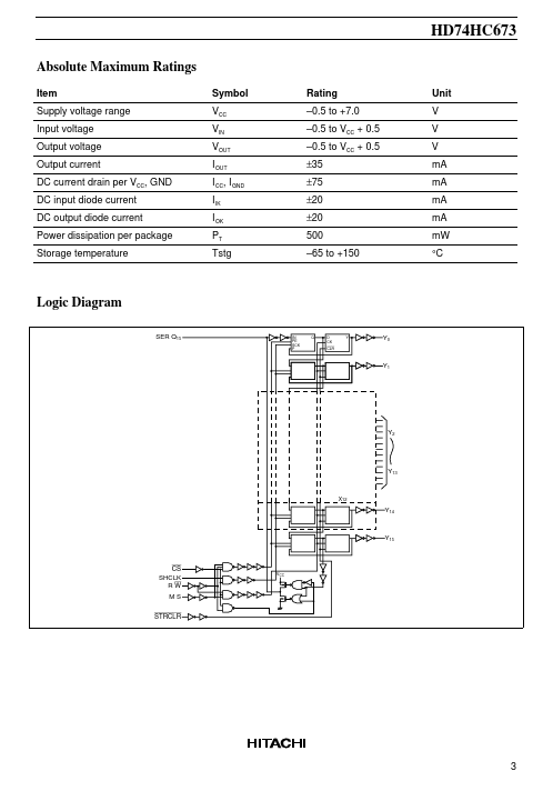
The HD74HC673 is a 16-bit shift register and a 16-bit storage register in a single 24-pin package. A threestate input/output (data I/O) port to the shift register allows serial entry and/or reading of data. The storage register is connected in a parallel data loop with the shift register and may be asynchronously cleared by taking the store-clear input low. The storage register may be parallel loaded with shift-register data to provide shift-register status via the parallel outputs. The shift register can be parallel loaded with the storage-register data upon command. A high logic level at the chip-select (CS) input disables both the shift-register clock and the storage register clock and places the data I/O in the high-impedance state.
 HD74HC673 Datasheet