Click to expand full text
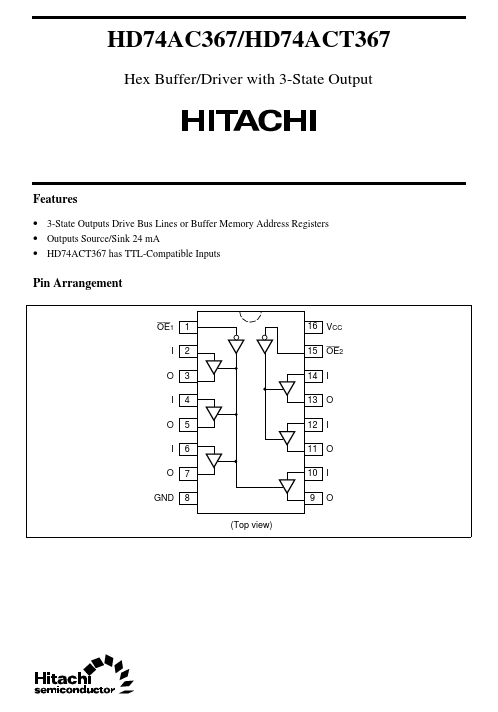
HD74AC367/HD74ACT367
Hex Buffer/Driver with 3-State Output
Features
• 3-State Outputs Drive Bus Lines or Buffer Memory Address Registers • Outputs Source/Sink 24 mA • HD74ACT367 has TTL-Compatible Inputs
Pin Arrangement
OE1 I O I O I O GND
1 2 3 4 5 6 7 8 (Top view)
16 VCC 15 OE2 14 I 13 O 12 I 11 O 10 I 9 O
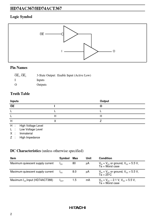
HD74AC367/HD74ACT367
Logic Symbol
OE
I
O
Pin Names
OE1, OE2 I O 3-State Output: Enable Input (Active Low) Inputs Outputs
Truth Table
Inputs OE L L H H L X Z : : : : High Voltage Level Low Voltage Level Immaterial High Impedance I L H X Output O L H Z
DC Characteristics (unless otherwise specified)
Item Maximum quiescent supply current Maximum quiescent supply current Maximum ICC/input (HD74ACT366) Symbol I CC I CC I CCT Max 80 8.0 1.
 HD74ACT367 Datasheet