Click to expand full text
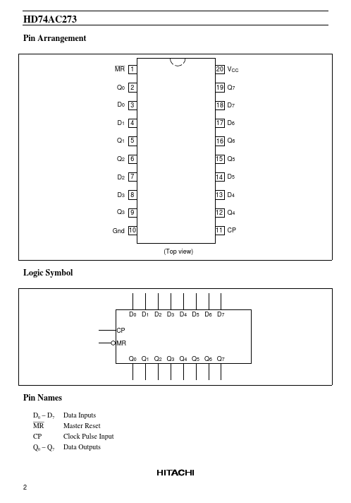
HD74AC273
Octal D Flip-Flop
Description
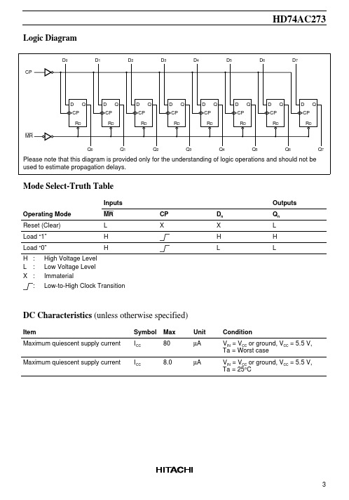
The HD74AC273 has eight edge-triggered D-type flip-flops with individual D inputs and Q outputs. The common buffered Clock (CP) and Master Reset (MR ) inputs load and reset (clear) all flip-flops simultaneously. The register is fully edge-triggered. The state of each D input, one setup time before the Low-to-High clock transition, is transferred to the corresponding flip-flops’s Q output All outputs will be forced Low independently of Clock or Data inputs by a Low voltage level on the MR input. The device is useful for applications where the true output only is required and the Clock and Master Reset are common to all storage elements.
 HD74AC273 Datasheet