Download the 2SJ245L datasheet PDF.
This datasheet also covers the 2SJ245 variant, as both devices belong to the same silicon p-channel mos fet family and are provided as variant models within a single manufacturer datasheet.
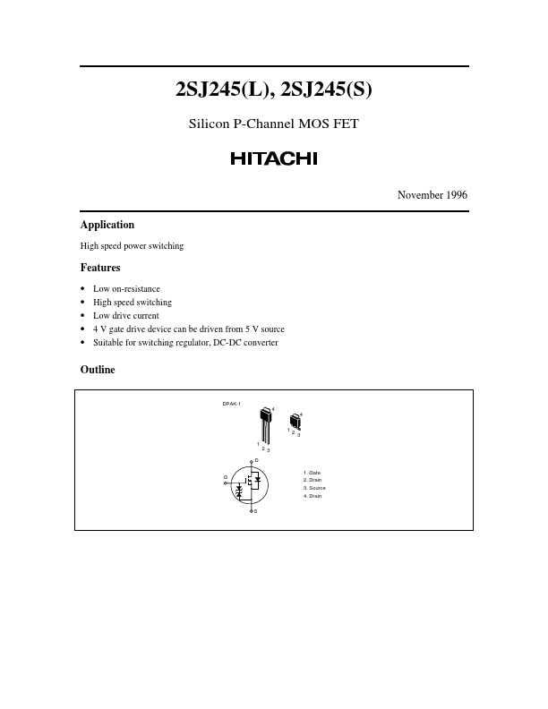
Key Features
Low on-resistance.
High speed switching.
Low drive current.
4 V gate drive device can be driven from 5 V source.
Suitable for switching regulator, DC-DC converter
Outline
DPAK-1
4 4
1 23
D
12 3
1. Gate
G
2. Drain
3. Source
4. Drain
S
November 1996
2SJ245(L), 2SJ245(S)
Absolute Maximum Ratings (Ta = 25°C)
Item Drain to source voltage Gate to source voltage Drain current Drain peak current Body to drain diode reverse drain current Channel.
Full PDF Text Transcription for 2SJ245L (Reference)
Note: Below is a high-fidelity text extraction (approx. 800 characters) for
2SJ245L. For precise diagrams, and layout, please refer to the original PDF.
2SJ245(L), 2SJ245(S) Silicon P-Channel MOS FET Application High speed power switching Features • Low on-resistance • High speed switching • Low drive current • 4 V gate d...
View more extracted text
on-resistance • High speed switching • Low drive current • 4 V gate drive device can be driven from 5 V source • Suitable for switching regulator, DC-DC converter Outline DPAK-1 4 4 1 23 D 12 3 1. Gate G 2. Drain 3. Source 4. Drain S November 1996 2SJ245(L), 2SJ245(S) Absolute Maximum Ratings (Ta = 25°C) Item Drain to source voltage Gate to source voltage Drain current Drain peak current Body to drain diode reverse drain current Channel dissipation Channel temperature Storage temperature Notes 1. PW ≤ 10 µs, duty cycle ≤ 1% 2.
 2SJ245L Datasheet