SI2305
Features
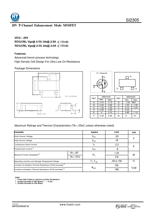
Advanced trench process technology High Density Cell Design For Ultra Low On-Resistance Package Dimensions
SOT-23(PACKAGE)
REF. A B C D E F
Millimeter Min. Max. 2.70 3.10 2.40 2.80 1.40 1.60 0.35 0.50 0 0.10 0.45 0.55
REF. G H K J L M
Millimeter Min. Max. 1.90 REF. 1.00 1.30 0.10 0.20 0.40 0.85 1.15 0° 10°
Maximum Ratings and Thermal Characteristics (TA = 25o C unless otherwise noted)
Parameter Drain-Source Voltage Gate-Source Voltage Continuous Drain Current Pulsed Drain Current
1)
Symbol
Limit
Unit
VDS VGS ID IDM
2)
-20 ±8 -2.2 -8 1.25 0.8 -55 to 150 100 166 o
TA = 25o TA = 75o C
2)
Maximum Power Dissipation
PD TJ, Tstg
Rth JA
W o
Operating Junction and Storage Temperature Range Junction-to-Ambient Thermal Resistance (PCB mounted)
Junction-to-Ambient Thermal Resistance (PCB mounted) 3)
C/W
Notes 1) Pulse width limited by maximum junction temperature. 2) Surface Mounted on FR4 Board, t v 5 sec. 3) Surface Mounted on FR4 Board.
Jin Yu...