HM4110
Features
- VDSS=0V/VGSS=±25V/ID=10A
RDS(ON)=5mΩ(max.)@VGS=10V
- Low Dense Cell Design
- Reliable and Rugged
- Advanced trench process technology
Applications
- Synchronous Rectification
- Power Management in Inverter System
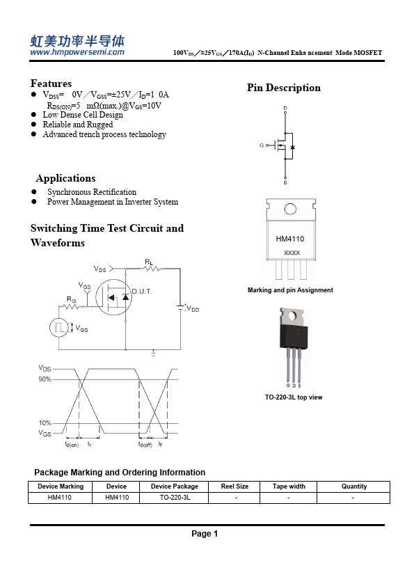
Switching Time Test Circuit and Waveforms
Pin Description
Marking and pin Assignment
TO-220-3L top view
Package Marking and Ordering Information
Device Marking HM4110
Device HM4110
Device Package TO-220-3L
Reel Size
- Tape width
- Page 1
Quantity
- HM4110
100VDS/±25VGS/170A(ID) N-Channel Enha ncement Mode MOSFET
Electrical Characteristics of CP Test (TA=25°C unless otherwise noted)
Symbol
Parameter
Test Conditions Min. Typ Max. Unit
Static Characteristics
BVDSS Drain-Source Breakdown Voltage VGS=0V,ID=250u A
IDSS
Zero Gate Voltage Drain Current
VDS=80V,VGS=0V TJ=85°C
1 30 u A
VGS(th) Gate Threshold Voltage
VDS=VGS,ID=250u...