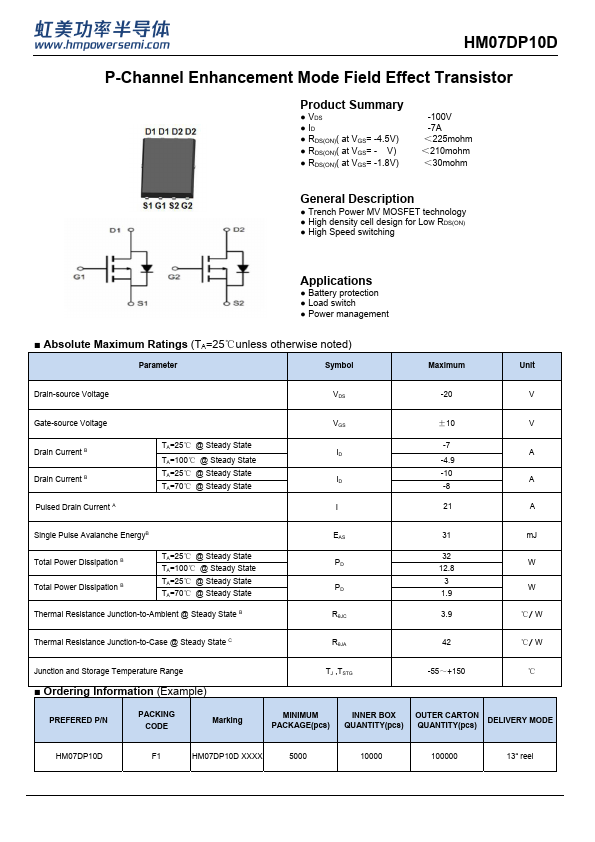
HM07DP10D
Description
- Trench Power MV MOSFET technology
- High density cell design for Low RDS(ON)
- High Speed switching
Applications
- Battery protection
- Load switch
- Power management
- Absolute Maximum Ratings (TA=25℃unless otherwise noted)
Parameter
Symbol
Maximum
Unit
Drain-source Voltage
-20
Gate-source Voltage Drain Current B Drain Current B Pulsed Drain Current A
TA=25℃ @ Steady State
TA=100℃ @ Steady State TA=25℃ @ Steady State TA=70℃ @ Steady State
Single Pulse Avalanche Energy B
Total Power Dissipation B Total Power Dissipation B
TA=25℃ @ Steady State TA=100℃ @ Steady State TA=25℃ @ Steady State TA=70℃ @ Steady State
Thermal Resistance Junction-to-Ambient @ Steady State B
VGS ID ID I '0 EAS PD PD RθJC
±10
-7 -4.9 -10 -8
32 12.8
3 1.9
V A A A m J W W ℃/ W
Thermal Resistance Junction-to-Case @ Steady State C
RθJA
℃/ W
Junction and Storage Temperature Range
- Ordering Information (Example)
PREFERED...