Click to expand full text
Real Time Clock - SPI Bus
2011/65/EU
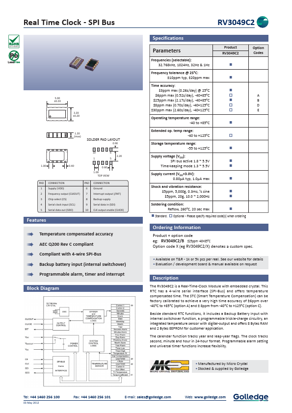
5.00 ±0.20
3.20 ±0.20
1.20 (max)
SOLDER PAD LAYOUT
0.90
10 6 2.20
15
1.00 0.40
0.60
1.00 TOP VIEW
PAD CONNECTION
PAD CONNECTION
1 Supply (VDD)
6 Ground
2 Frequency output (CLKOUT) 7 Interrupt output (/INT)
3 Chip select (CS)
8 Backup supply
4 Serial clock input (SCL)
9 Serial data in (SDI)
5 Serial data out (SDO)
10 CLK output enable (CLKOE)
Features
Temperature compensated accuracy AEC Q200 Rev C compliant Compliant with 4-wire SPI-Bus Backup battery input (internal switchover) Programmable alarm, timer and interrupt
Block Diagram
RV3049C2
Specifications
Parameters
Frequencies (selectable): 32.
 RV3049C2 Datasheet