GD751SD
Description
S U R F A C E M O U N T, S C H O T T K Y B A R R I E R D I O D E V O LT A G E 4 0 V, C U R R E N T 0 . 0 3 A
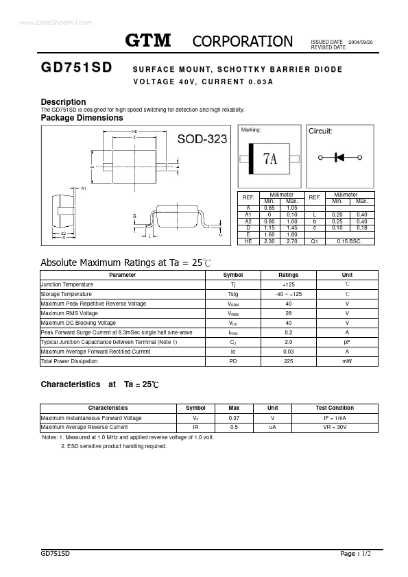
Package Dimensions
The GD751SD is designed for high speed switching for detection and high reliability.
REF. A A1 A2 D E HE
Millimeter Min. Max. 0.85 1.05 0 0.10 0.80 1.00 1.15 1.45 1.60 1.80 2.30 2.70
REF. L b c Q1
Millimeter Min. Max. 0.20 0.25 0.10 0.40 0.40 0.18
0.15 BSC.
Parameter Junction Temperature Storage Temperature Maximum Peak Repetitive Reverse Voltage Maximum RMS Voltage Maximum DC Blocking Voltage Peak Forward Surge Current at 8.3m Sec single half sine-wave Typical Junction Capacitance between Terminal (Note 1) Maximum Average Forward Rectified Current Total Power Dissipation
Symbol Tj Tstg VRRM VRMS VDC IFSM CJ Io PD
Ratings +125 -40 ~ +125 40 28 40 0.2 2.0 0.03 225
Unit
V V V A p F A m W
Characteristics at Ta = 25
Symbol VF IR Max 0.37 0.5 Unit V u A Test Condition IF = 1m A VR = 30V
Characteristics Maximum Instantaneous Forward Voltage...