GD420SD
Description
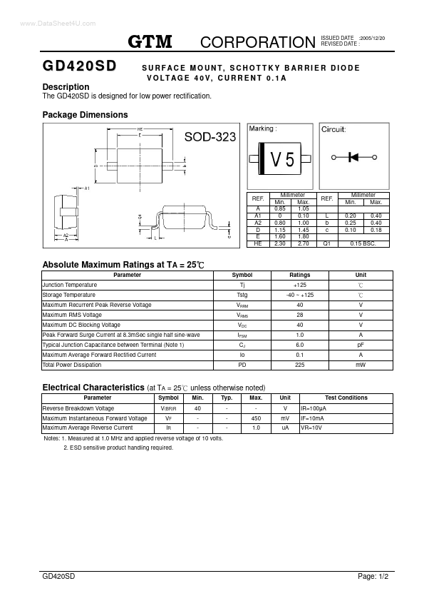
Package Dimensions
ISSUED DATE :2005/12/20 REVISED DATE :
S U R F A C E M O U N T, S C H O T T K Y B A R R I E R D I O D E V O LT A G E 4 0 V, C U R R E N T 0 . 1 A
The GD420SD is designed for low power rectification.
REF. A A1 A2 D E HE
Millimeter Min. Max. 0.85 1.05 0 0.10 0.80 1.00 1.15 1.45 1.60 1.80 2.30 2.70
REF. L b c Q1
Millimeter Min. Max. 0.20 0.25 0.10 0.40 0.40 0.18
0.15 BSC.
Absolute Maximum Ratings at TA = 25
Parameter Junction Temperature Storage Temperature Maximum Recurrent Peak Reverse Voltage Maximum RMS Voltage Maximum DC Blocking Voltage Peak Forward Surge Current at 8.3m Sec single half sine-wave Typical Junction Capacitance between Terminal (Note 1) Maximum Average Forward Rectified Current Total Power Dissipation Symbol Tj Tstg VRRM VRMS VDC IFSM CJ Io PD Ratings +125 -40 ~ +125 40 28 40 1.0 6.0 0.1 225 V V V A p F A m W Unit
Electrical Characteristics (at TA = 25
Parameter Reverse Breakdown Voltage Maximum Instantaneous Forward Voltage...