Download the BZX84C18 datasheet PDF.
This datasheet also covers the BZX84C2V4-GOOD variant, as both devices belong to the same surface mount zener diodes family and are provided as variant models within a single manufacturer datasheet.
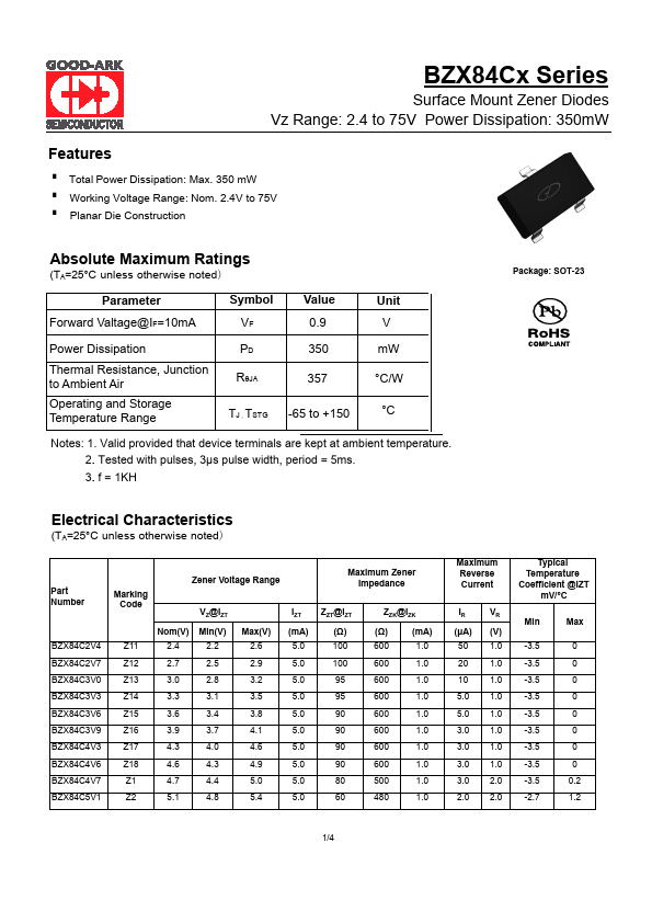
Key Features
Total Power Dissipation: Max. 350 mW.
Working Voltage Range: Nom. 2.4V to 75V.
Planar Die Construction
Absolute Maximum Ratings
(TA=25°C unless otherwise noted)
Parameter Forward Valtage@IF=10mA
Symbol VF
Value 0.9
Unit V
Power Dissipation
Thermal Resistance, Junction to Ambient Air
Operating and Storage Temperature Range
PD RθJA TJ,TSTG
350 357 -65 to +150
mW °C/W
°C
Notes: 1. Valid provided that device terminals are kept at ambient temperature. 2. Tested with pulses,.
Full PDF Text Transcription for BZX84C18 (Reference)
Note: Below is a high-fidelity text extraction (approx. 800 characters) for
BZX84C18. For precise diagrams, and layout, please refer to the original PDF.
BZX84Cx Series Surface Mount Zener Diodes Vz Range: 2.4 to 75V Power Dissipation: 350mW Features ■ Total Power Dissipation: Max. 350 mW ■ Working Voltage Range: Nom. 2.4V...
View more extracted text
otal Power Dissipation: Max. 350 mW ■ Working Voltage Range: Nom. 2.4V to 75V ■ Planar Die Construction Absolute Maximum Ratings (TA=25°C unless otherwise noted) Parameter Forward Valtage@IF=10mA Symbol VF Value 0.9 Unit V Power Dissipation Thermal Resistance, Junction to Ambient Air Operating and Storage Temperature Range PD RθJA TJ,TSTG 350 357 -65 to +150 mW °C/W °C Notes: 1. Valid provided that device terminals are kept at ambient temperature. 2. Tested with pulses, 3μs pulse width, period = 5ms. 3.
 BZX84C18 Datasheet