G110N06
Description
The G110N06 is N-channel MOS Field Effect Transistor designed for high current switching applications. Rugged EAS capability and ultra low RDS(ON) is suitable for PWM, load switching applications.
Features
- VDSS RDS(ON) ID
@ 10V(Typ)
55V
5.2 mΩ 110A
- Ultra Low On-Resistance
- High UIS and UIS 100% Test
Application
- Hard Switched and High Frequency Circuits
- Uninterruptible Power Supply
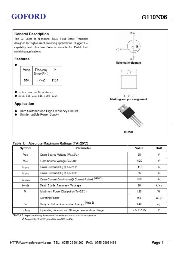
Schematic diagram Marking and pin assignment
Table 1. Absolute Maximum Ratings (TA=25℃)
Symbol
Parameter
Drain-Source Voltage (VGS=0V)
Gate-Source Voltage (VDS=0V)
ID (DC) ID (DC) IDM (pluse) dv/dt
Drain Current (DC) at Tc=25℃ Drain Current (DC) at Tc=100℃ Drain Current-Continuous@ Current-Pulsed (Note 1) Peak Diode Recovery Voltage
Maximum Power Dissipation(Tc=25℃)
Derating Factor
Single Pulse Avalanche Energy (Note 2)
TJ,TSTG
Operating Junction and Storage Temperature Range
Notes 1.Repetitive Rating: Pulse width limited by maximum junction...