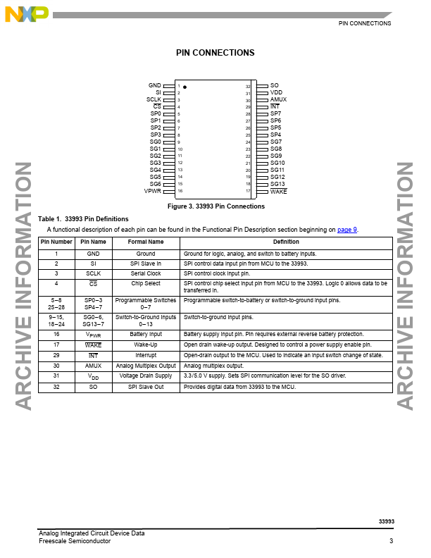
Description
of each pin can be found in the Functional Pin Description section beginning on page 9.
8 25
28 9
15, 18
24
16 17 29 30 31 32
GND SI
SCLK CS
SP0
3 SP4
7 SG0
6, SG13
7 VPWR WAKE
INT AMUX
VDD SO
Ground SPI Slave In Serial Clock Chip Select
Programmable Switches 0
7
Switch-to-Ground Inputs 0
13
Battery Input
Ground for logic, analog, and switch
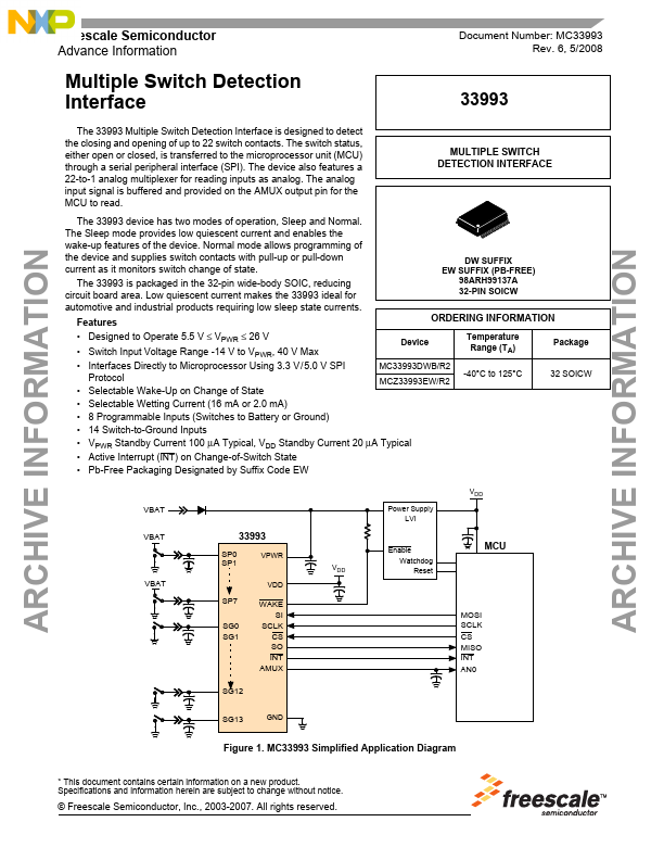
Features
- a 22-to-1 analog multiplexer for reading inputs as analog. The analog input signal is buffered and provided on the AMUX output pin for the MCU to read.
 33993 Datasheet