Datasheet Details
| Part number | NDS9933A |
|---|---|
| Manufacturer | Fairchild |
| File Size | 191.77 KB |
| Description | Dual P-Channel MOSFET |
| Datasheet |
 NDS9933A Datasheet NDS9933A Datasheet
|
|
|
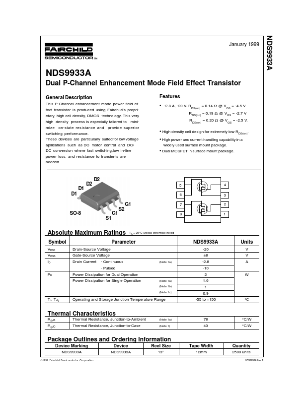
This P-Channel enhancement mode power field effect transistor is produced using Fairchild’s proprietary, high cell density, DMOS technology.
This very high density process is especially tailored to minimize on-state resistance and provide superior switching performance.
| Part number | NDS9933A |
|---|---|
| Manufacturer | Fairchild |
| File Size | 191.77 KB |
| Description | Dual P-Channel MOSFET |
| Datasheet |
NDS9933A Datasheet
|
|
|
|