Datasheet Details
| Part number | NDS352AP |
|---|---|
| Manufacturer | Fairchild |
| File Size | 78.57 KB |
| Description | P-Channel Logic Level Enhancement Mode Field Effect Transistor |
| Datasheet |
 NDS352AP Datasheet NDS352AP Datasheet
|
|
|
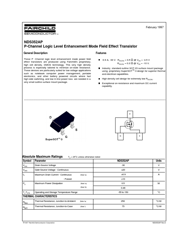
These P -Channel logic level enhancement mode power field effect transistors are produced using Fairchild's proprietary, high cell density, DMOS technology.
This very high density process is especially tailored to minimize on-state resistance.
| Part number | NDS352AP |
|---|---|
| Manufacturer | Fairchild |
| File Size | 78.57 KB |
| Description | P-Channel Logic Level Enhancement Mode Field Effect Transistor |
| Datasheet |
NDS352AP Datasheet
|
|
|
|