Click to expand full text
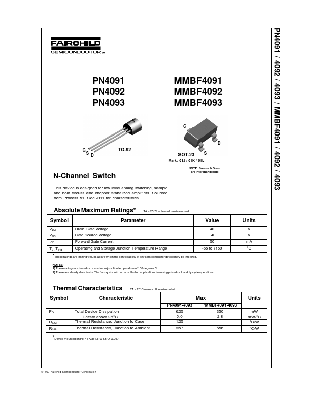
PN4091 / 4092 / 4093 / MMBF4091 / 4092 / 4093
PN4091 PN4092 PN4093
MMBF4091 MMBF4092 MMBF4093
G
D G S
TO-92
D
SOT-23
S
Mark: 61J / 61K / 61L
NOTE: Source & Drain are interchangeable
N-Channel Switch
This device is designed for low level analog switching, sample and hold circuits and chopper stabalized amplifiers. Sourced from Process 51. See J111 for characteristics.
Absolute Maximum Ratings*
Symbol
VDG VGS IGF TJ ,Tstg Drain-Gate Voltage Gate-Source Voltage Forward Gate Current
TA = 25°C unless otherwise noted
Parameter
Value
40 - 40 50 -55 to +150
Units
V V mA °C
Operating and Storage Junction Temperature Range
*These ratings are limiting values above which the serviceability of any semiconductor device may be impaired.
 PN4092 Datasheet