The following content is an automatically extracted verbatim text
from the original manufacturer datasheet and is provided for reference purposes only.
View original datasheet text
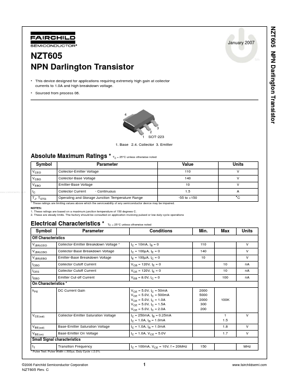
NZT605 NPN Darlington Transistor
January 2007
NZT605
NPN Darlington Transistor
• This device designed for applications requiring extremely high gain at collector currents to 1.0A and high breakdown voltage. • Sourced from process 06.
4
3 2 1
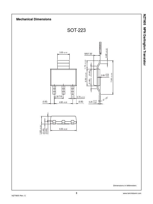
SOT-223
1. Base 2.4. Collector 3. Emitter
Absolute Maximum Ratings * T
Symbol
VCEO VCBO VEBO
www.DataSheet4U.com
C
= 25°C unless otherwise noted
Parameter
Collector-Emitter Voltage Collector-Base Voltage Emitter-Base Voltage Collector Current - Continuous
Value
110 140 10 1.5 -55 to +150
Units
V V V A °C
IC TJ, TSTG
Operating and Storage Junction Temperature Range
* These ratings are limiting values above which the serviceability of any semiconductor device may be impaired. NOTES: 1.
 NZT605 Datasheet