The following content is an automatically extracted verbatim text
from the original manufacturer datasheet and is provided for reference purposes only.
View original datasheet text
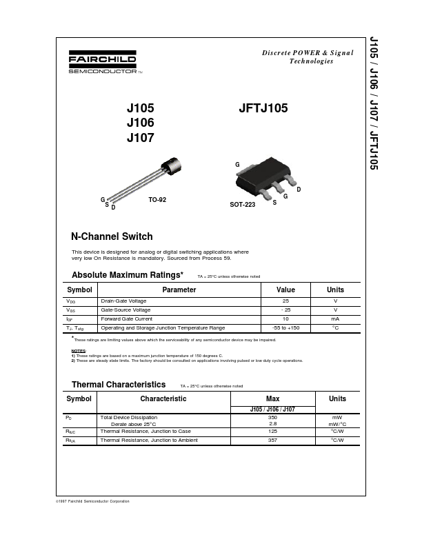
J105 / J106 / J107 / JFTJ105
Discrete POWER & Signal Technologies
J105 J106 J107
JFTJ105
G
D G S D
TO-92
G
SOT-223
S
N-Channel Switch
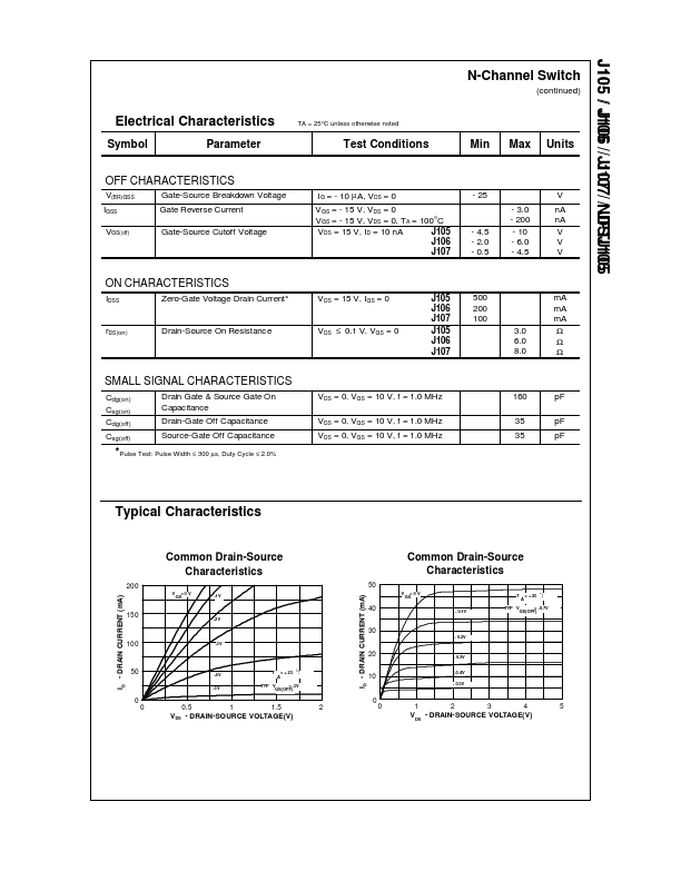
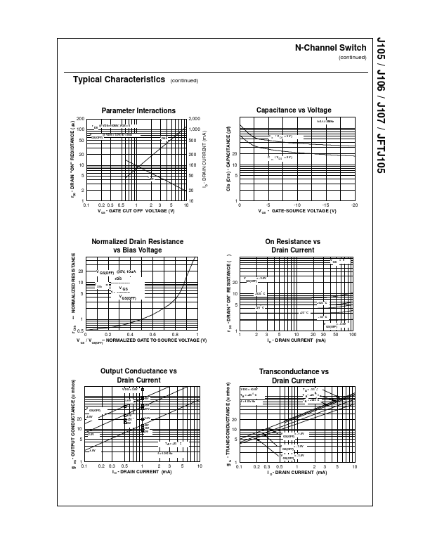
This device is designed for analog or digital switching applications where very low On Resistance is mandatory. Sourced from Process 59.
Absolute Maximum Ratings*
Symbol
VDG VGS IGF TJ, Tstg Drain-Gate Voltage Gate-Source Voltage Forward Gate Current
TA = 25°C unless otherwise noted
Parameter
Value
25 - 25 10 -55 to +150
Units
V V mA °C
Operating and Storage Junction Temperature Range
*These ratings are limiting values above which the serviceability of any semiconductor device may be impaired.
NOTES: 1) These ratings are based on a maximum junction temperature of 150 degrees C. 2) These are steady state limits.
 JFTJ105 Datasheet