The following content is an automatically extracted verbatim text
from the original manufacturer datasheet and is provided for reference purposes only.
View original datasheet text
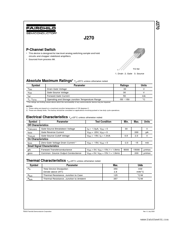
J270
J270
P-Channel Switch
• This device is designed for low level analog switching sample and hold circuits and chopper stabilized amplifiers. • Sourced from process 88.
1
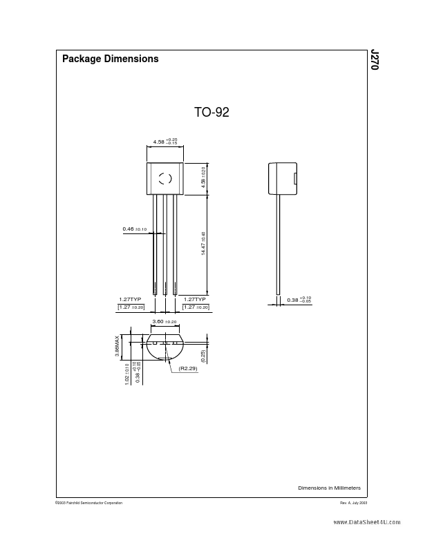
TO-92
1. Drain 2. Gate 3. Source
Absolute Maximum Ratings* Ta=25°C unless otherwise noted
Symbol VDG VGS IGF TJ, TSTG Parameter Drain-Gate Voltage Gate-Source Voltage Forward Gate Current Operating and Storage Junction Temperature Range Ratings -30 30 50 -55 ~ 150 Units V V mA °C
* This ratings are limiting values above which the serviceability of any semiconductor device may be impaired. NOTES: 1) These rating are based on a maximum junction temperature of 150 degrees C. 2) These are steady limits. The factory should be consulted on applications involving pulsed or low duty cycle operations.
 J270 Datasheet