Full PDF Text Transcription for FMBA14 (Reference)
Note: Below is a high-fidelity text extraction (approx. 800 characters) for
FMBA14. For precise diagrams, and layout, please refer to the original PDF.
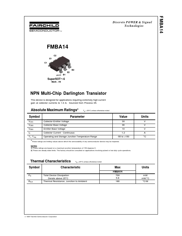
FMBA14 Discrete POWER & Signal Technologies FMBA14 C2 E1 C1 B2 E2 pin #1 B1 SuperSOT™-6 Mark: .1N NPN Multi-Chip Darlington Transistor This device is designed for applica...
View more extracted text
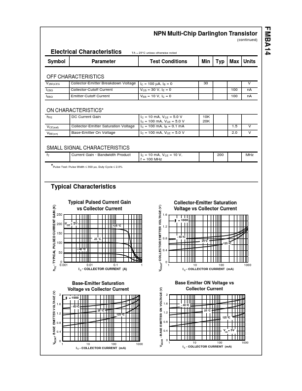
N Multi-Chip Darlington Transistor This device is designed for applications requiring extremely high current gain at collector currents to 1.0 A. Sourced from Process 05. Absolute Maximum Ratings* Symbol VCES VCBO VEBO IC TJ, Tstg Collector-Emitter Voltage Collector-Base Voltage Emitter-Base Voltage Collector Current - Continuous TA = 25°C unless otherwise noted Parameter Value 30 30 10 1.2 -55 to +150 Units V V V A °C Operating and Storage Junction Temperature Range *These ratings are limiting values above which the serviceability of any semiconductor device may be impaired. NOTES: 1) These ratings are based on a maximum
 FMBA14 Datasheet