Datasheet Details
| Part number | FIN1047 |
|---|---|
| Manufacturer | Fairchild (now onsemi) |
| File Size | 315.35 KB |
| Description | 3.3V LVDS 4-Bit Flow-Through |
| Datasheet |
 FIN1047 Datasheet FIN1047 Datasheet
|
|
|
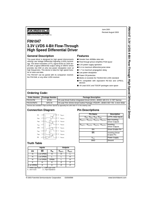
This quad driver is designed for high speed interconnects utilizing Low Voltage Differential Signaling (LVDS) technology.
| Part number | FIN1047 |
|---|---|
| Manufacturer | Fairchild (now onsemi) |
| File Size | 315.35 KB |
| Description | 3.3V LVDS 4-Bit Flow-Through |
| Datasheet |
FIN1047 Datasheet
|
|
|
|
| Part Number | Description | Manufacturer |
|---|---|---|
| FIN1001 | High-Speed Differential Driver | ON Semiconductor |
| FIN1002 | High-Speed Differential Reciever | ON Semiconductor |
| FIN1019 | 3.3V LVDS High Speed Differential Driver/Receiver | ON Semiconductor |
| FinePix S5100 | Manual | Fujifilm |
| FinePix S5500 | Manual | Fujifilm |
| Part Number | Description |
|---|---|
| FIN1048 | 3.3V LVDS 4-Bit Flow-Through High Speed Differential Receiver |
| FIN1049 | LVDS Dual Line Driver |
| FIN1001 | 3.3V LVDS 1-Bit High Speed Differential Driver |
| FIN1002 | LVDS 1-Bit High Speed Differential Receiver |
| FIN1017 | 3.3V LVDS 1-Bit High Speed Differential Driver |
The following content is an automatically extracted verbatim text from the original manufacturer datasheet and is provided for reference purposes only.