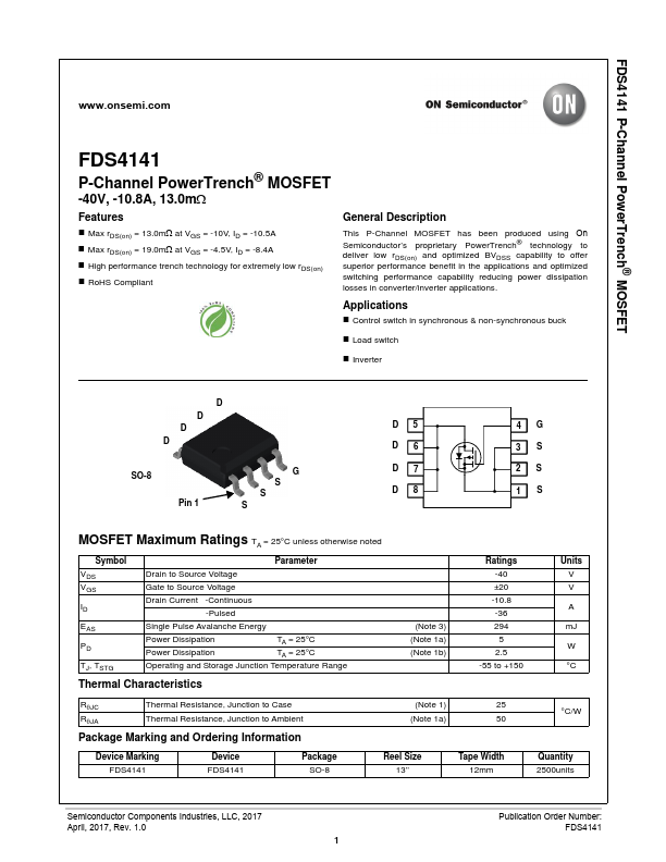
Datasheet4U Logo Datasheet4U.com

FDS4141 - P-Channel MOSFET

General Description

This P-Channel MOSFET has been produced using On Semiconductor’s proprietary PowerTrench® technology to deliver low rDS(on) and optimized BVDSS capability to offer superior performance benefit in the applications and optimized switching performance capability reducing power dissipation losses in converter/inverter applications.

Applications „ Control switch in synchronous & non-synchronous buck „ Load switch „ Inverter D D D D SO-8 Pin 1 G S S S D5 D6 D7 D8 4G 3S 2S 1S MOSFET Maximum Ratings TA = 25°C unless otherwise noted Symbol VDS VGS ID EAS PD TJ, TSTG Parameter Drain to Source Voltage Gate to Source Voltage Drain Current -Continuous -Pulsed Single Pulse Avalanche Energy Power Dissipation TA = 25°C Power Dissipation TA = 25°C Operating and Storage Junction Temperature Range Thermal Characteristics (Note 3) (Note 1a) (Note 1b) Ratings -40 ±20 -10.8 -36 294 5 2.5 -55 to +150 Units V V A mJ W °C RθJC RθJA Thermal Resistance, Junction to Case Thermal Resistance, Junction to Ambient Package Marking and Ordering Information (Note 1) 25 (Note 1a) 50 °C/W Device Marking FDS4141 Device FDS4141 Package SO-8 Reel Size 13’’ Tape Width 12mm Quantity 2500units Semiconductor Components Industries, LLC, 2017 April, 2017, Rev.

1.0 1 Publication Order Number: FDS4141 FDS4141 P-Channel PowerTrench® MOSFET Electrical Characteristics TJ = 25°C unless otherwise noted Symbol Parameter Test Conditions Min Typ Max Units Off Characteristics BVDSS ∆BVDSS ∆TJ IDSS IGSS Drain to Source Breakdown Voltage Breakdown Voltage Temperature Coefficient Zero Gate Voltage Drain Current Gate to Source Leakage Current ID = -250µA, V

Overview

FDS4141 P-Channel PowerTrench® MOSFET www.onsemi.com FDS4141 P-Channel PowerTrench® MOSFET -40V, -10.8A, 13.

Key Features

  • Max rDS(on) = 13.0mΩ at VGS = -10V, ID = -10.5A.
  • Max rDS(on) = 19.0mΩ at VGS = -4.5V, ID = -8.4A.
  • High performance trench technology for extremely low rDS(on).
  • RoHS Compliant General.