The following content is an automatically extracted verbatim text
from the original manufacturer datasheet and is provided for reference purposes only.
View original datasheet text
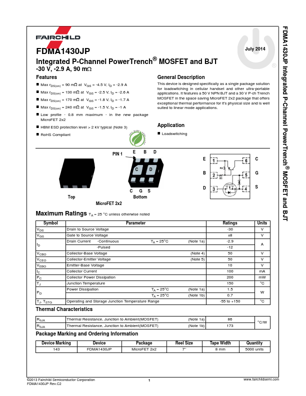
FDMA1430JP Integrated P-Channel PowerTrench® MOSFET and BJT
FDMA1430JP
Integrated P-Channel PowerTrench® MOSFET and BJT
-30 V, -2.9 A, 90 mΩ
July 2014
Features
Max rDS(on) = 90 mΩ at VGS = -4.5 V, ID = -2.9 A Max rDS(on) = 130 mΩ at VGS = -2.5 V, ID = -2.6 A Max rDS(on) = 170 mΩ at VGS = -1.8 V, ID = -1.7 A Max rDS(on) = 240 mΩ at VGS = -1.5 V, ID = -1 A Low profile - 0.8 mm maximum - in the new package
MicroFET 2x2
HBM ESD protection level > 2 kV typical (Note 3)
RoHS Compliant
General Description
This device is designed specifically as a single package solution for loadswitching in cellular handset and other ultra-portable applications.
 FDMA1430JP Datasheet