Datasheet Details
| Part number | 74VCXR162601 |
|---|---|
| Manufacturer | Fairchild (now onsemi) |
| File Size | 142.96 KB |
| Description | Low Voltage 18-Bit Universal Bus Transceivers |
| Datasheet |
 74VCXR162601 Datasheet 74VCXR162601 Datasheet
|
|
|
Download the 74VCXR162601 datasheet PDF. This datasheet also covers the 74VCXR variant, as both devices belong to the same low voltage 18-bit universal bus transceivers family and are provided as variant models within a single manufacturer datasheet.
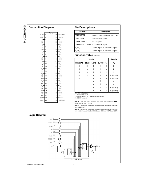
The VCXR162601, 18-bit universal bus transceiver, combines D-type latches and D-type flip-flops to allow data flow in transparent, latched, and clocked modes.
Data flow in each direction is controlled by output-enable (OEAB and OEBA), latch-enable (LEAB and LEBA), and clock (CLKAB and CLKBA) inputs.
| Part number | 74VCXR162601 |
|---|---|
| Manufacturer | Fairchild (now onsemi) |
| File Size | 142.96 KB |
| Description | Low Voltage 18-Bit Universal Bus Transceivers |
| Datasheet |
74VCXR162601 Datasheet
|
|
|
|
| Part Number | Description | Manufacturer |
|---|---|---|
| 74VCX162244 | LOW VOLTAGE CMOS 16-BIT BUS BUFFER | ST Microelectronics |
| 74VCX16240 | LOW VOLTAGE CMOS 16-BIT BUS BUFFER | STMicroelectronics |
| 74VCX16240 | Low-Voltage 1.8/2.5/3.3V 16-Bit Buffer | ON Semiconductor |
| 74VCX16244 | Low-Voltage 1.8V/2.5V/3.3V 16-Bit Buffer | ON Semiconductor |
| 74VCX16245 | Low-Voltage 1.8/2.5/3.3V 16-Bit Transceiver | ON Semiconductor |
| Part Number | Description |
|---|---|
| 74VCX00 | Low Voltage Quad 2-Input NAND Gate |
| 74VCX08 | Low Voltage Quad 2-Input AND Gate |
| 74VCX132 | Low Voltage Quad 2-Input NAND Gate |
| 74VCX162240 | Low Voltage 16-Bit Inverting Buffer/Line Driver |
| 74VCX162244 | Low Voltage 16-Bit Buffer/Line Driver |
The following content is an automatically extracted verbatim text from the original manufacturer datasheet and is provided for reference purposes only.