The following content is an automatically extracted verbatim text
from the original manufacturer datasheet and is provided for reference purposes only.
View original datasheet text
74LCX16500 Low Voltage 18-Bit Universal Bus Transceivers with 5V Tolerant Inputs and Outputs
March 1995 Revised April 1999
74LCX16500 Low Voltage 18-Bit Universal Bus Transceivers with 5V Tolerant Inputs and Outputs
General Description
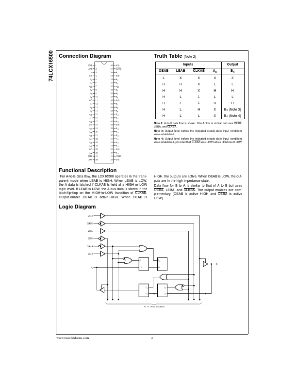
These 18-bit universal bus transceivers combine D-type latches and D-type flip-flops to allow data flow in transparent, latched, and clocked modes. Data flow in each direction is controlled by output-enable (OEAB and OEBA), latch-enable (LEAB and LEBA), and clock (CLKAB and CLKBA) inputs. The LCX16500 is designed for low voltage (2.5V or 3.3V) VCC applications with the capability of interfacing to a 5V signal environment. The LCX16500 is fabricated with an advanced CMOS technology to achieve high speed operation while maintaining CMOS low power.
 74LCX16500 Datasheet