Datasheet Details
| Part number | M14D2561616A-2.5BG2S |
|---|---|
| Manufacturer | ESMT (Elite Semiconductor Microelectronics Technology) |
| File Size | 1.57 MB |
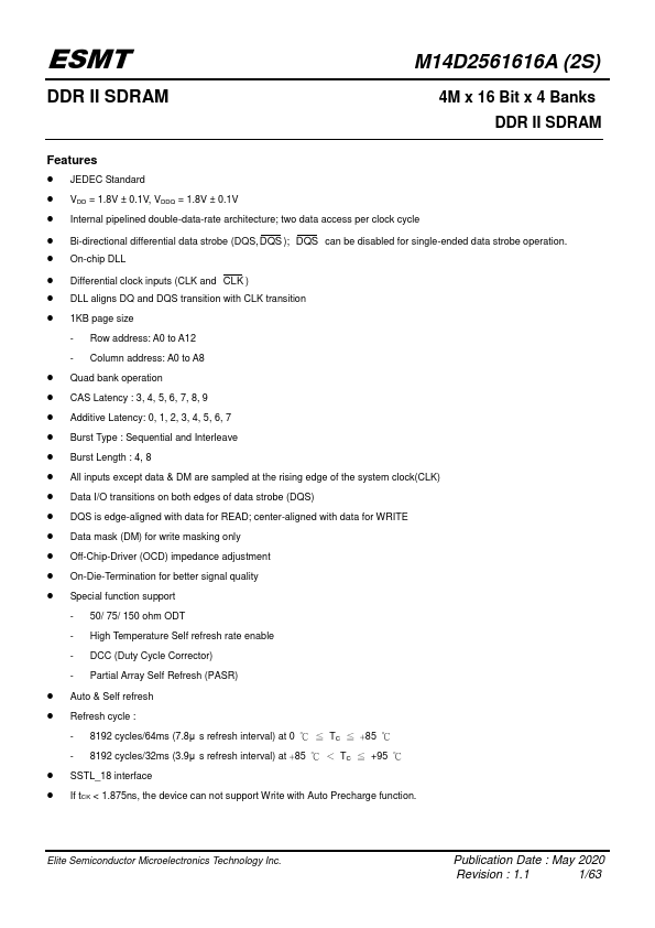
| Description | 4M x 16 Bit x 4 Banks DDR II SDRAM |
| Datasheet |
 M14D2561616A-2.5BG2S Datasheet M14D2561616A-2.5BG2S Datasheet
|
|
|
Download the M14D2561616A-2.5BG2S datasheet PDF. This datasheet also covers the M14D2561616A variant, as both devices belong to the same 4m x 16 bit x 4 banks ddr ii sdram family and are provided as variant models within a single manufacturer datasheet.
| Part number | M14D2561616A-2.5BG2S |
|---|---|
| Manufacturer | ESMT (Elite Semiconductor Microelectronics Technology) |
| File Size | 1.57 MB |
| Description | 4M x 16 Bit x 4 Banks DDR II SDRAM |
| Datasheet |
M14D2561616A-2.5BG2S Datasheet
|
|
|
|
| Part Number | Description | Manufacturer |
|---|---|---|
| M140NWR1-R0 | TFT LCD | IVO |
| M140NWR2-R0 | TFT LCD | IVO |
| M140NWR2-R1 | TFT LCD | IVO |
| M140NWR2-R2 | TFT LCD | IVO |
| M141-X76C | TFT Color LCD | IMES |
| Part Number | Description |
|---|---|
| M14D2561616A-2.5BG2C | 4M x 16 Bit x 4 Banks DDR II SDRAM |
| M14D2561616A-2.5BBG2S | 4M x 16 Bit x 4 Banks DDR II SDRAM |
| M14D2561616A-2.5BIG2C | DDR II SDRAM |
| M14D2561616A-1.5BG2C | 4M x 16 Bit x 4 Banks DDR II SDRAM |
| M14D2561616A-1.5BG2S | 4M x 16 Bit x 4 Banks DDR II SDRAM |
The following content is an automatically extracted verbatim text from the original manufacturer datasheet and is provided for reference purposes only.