Datasheet4U Logo Datasheet4U.com

PI6CG188Q - 8-Output PCIe Gen 4 Clock Generator

Description

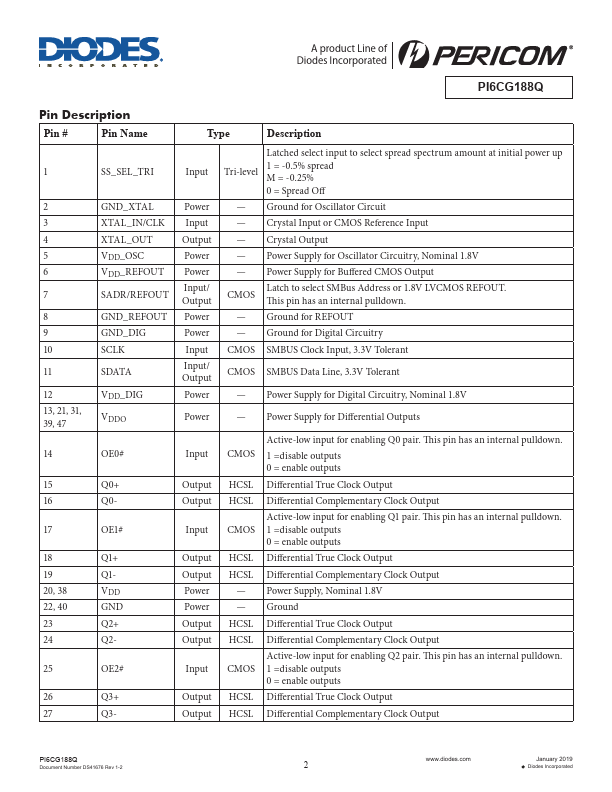
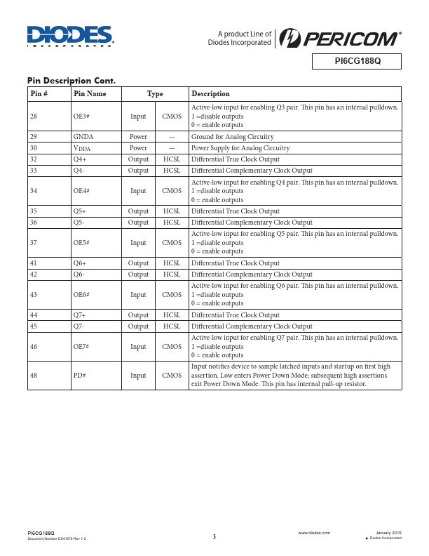
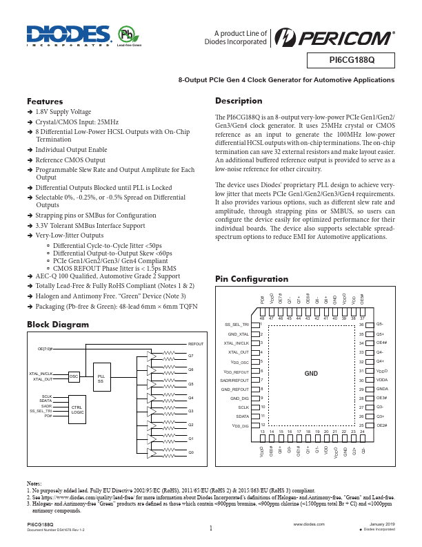
The PI6CG188Q is an 8-output very-low-power PCIe Gen1/Gen2/ Gen3/Gen4 clock generator.

It uses 25MHz crystal or CMOS reference as an input to generate the 100MHz low-power differential HCSL outputs with on-chip terminations.

Features

  • ÎÎ1.8V Supply Voltage ÎÎCrystal/CMOS Input: 25MHz ÎÎ8 Differential Low-Power HCSL Outputs with On-Chip Termination ÎÎIndividual Output Enable ÎÎReference CMOS Output ÎÎProgrammable Slew Rate and Output Amplitute for Each Output ÎÎDifferential Outputs Blocked until PLL is Locked ÎÎSelectable 0%, -0.25%, or -0.5% Spread on Differential Outputs ÎÎStrapping pins or SMBus for Configuration ÎÎ3.3V Tolerant SMBus Interface Support ÎÎVery-Low-Jitter Outputs àà Differential Cycle-to-Cycle Jitter.

📥 Download Datasheet

Datasheet preview – PI6CG188Q

Datasheet Details

Part number PI6CG188Q
Manufacturer DIODES
File Size 1.06 MB
Description 8-Output PCIe Gen 4 Clock Generator
Datasheet download datasheet PI6CG188Q Datasheet
Additional preview pages of the PI6CG188Q datasheet.
Other Datasheets by Diodes

Full PDF Text Transcription

Click to expand full text
Pb Lead-free Green A product Line of Diodes Incorporated PI6CG188Q 8-Output PCIe Gen 4 Clock Generator for Automotive Applications Features ÎÎ1.8V Supply Voltage ÎÎCrystal/CMOS Input: 25MHz ÎÎ8 Differential Low-Power HCSL Outputs with On-Chip Termination ÎÎIndividual Output Enable ÎÎReference CMOS Output ÎÎProgrammable Slew Rate and Output Amplitute for Each Output ÎÎDifferential Outputs Blocked until PLL is Locked ÎÎSelectable 0%, -0.25%, or -0.5% Spread on Differential Outputs ÎÎStrapping pins or SMBus for Configuration ÎÎ3.3V Tolerant SMBus Interface Support ÎÎVery-Low-Jitter Outputs àà Differential Cycle-to-Cycle Jitter <50ps àà Differential Output-to-Output Skew <60ps àà PCIe Gen1/Gen2/Gen3/ Gen4 Compliant àà CMOS REFOUT Phase Jitter is < 1.
Published: |