Datasheet4U Logo Datasheet4U.com

PI6CB184Q - 4-Output PCIe Gen 4 Clock Buffer

Datasheet Summary

Description

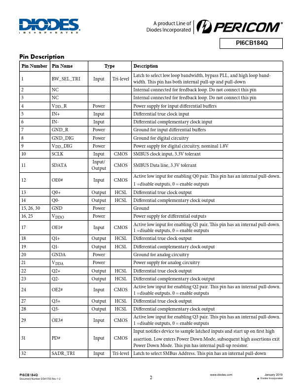
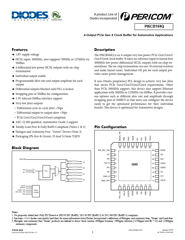
The PI6CB184Q is an 4-output very low power PCIe Gen1/Gen2/ Gen3/Gen4 clock buffer.

It takes an reference input to fanout four 100MHz low power differential HCSL outputs with on-chip terminations.

The on-chip termination can save 16 external resistors and make layout easier.

Features

  • ÎÎ1.8V supply voltage ÎÎHCSL input: 100MHz, also suppport 50MHz or 125MHz via SMBus ÎÎ4 differential low power HCSL outputs with on-chip termination ÎÎIndividual output enable ÎÎProgrammable Slew rate and output amplitute for each output ÎÎDifferential outputs blocked until PLL is locked ÎÎStrapping pins or SMBus for configuration; ÎÎ3.3V tolerant SMBus interface support ÎÎVery low jitter outputs yyDifferential cycle-to-cycle jitter.

📥 Download Datasheet

Datasheet preview – PI6CB184Q

Datasheet Details

Part number PI6CB184Q
Manufacturer DIODES
File Size 1.07 MB
Description 4-Output PCIe Gen 4 Clock Buffer
Datasheet download datasheet PI6CB184Q Datasheet
Additional preview pages of the PI6CB184Q datasheet.
Other Datasheets by Diodes

Full PDF Text Transcription

Click to expand full text
Pb Lead-free Green A product Line of Diodes Incorporated PI6CB184Q 4-Output PCIe Gen 4 Clock Buffer for Automotive Applications Features ÎÎ1.8V supply voltage ÎÎHCSL input: 100MHz, also suppport 50MHz or 125MHz via SMBus ÎÎ4 differential low power HCSL outputs with on-chip termination ÎÎIndividual output enable ÎÎProgrammable Slew rate and output amplitute for each output ÎÎDifferential outputs blocked until PLL is locked ÎÎStrapping pins or SMBus for configuration; ÎÎ3.3V tolerant SMBus interface support ÎÎVery low jitter outputs yyDifferential cycle-to-cycle jitter <50ps yyDifferential output-to-output skew <50ps yyPCIe Gen1/Gen2/Gen3/Gen4 compliant ÎÎAEC-Q 100 qualified, Automotive Grade 2 support ÎÎTotally Lead-Free & Fully RoHS Compliant (Notes 1 & 2) ÎÎHalogen and Antimony Free.
Published: |