The following content is an automatically extracted verbatim text
from the original manufacturer datasheet and is provided for reference purposes only.
View original datasheet text
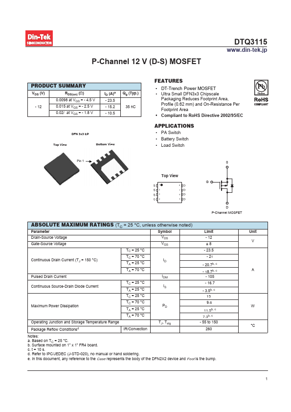
3�&KDQQHO�12�9��'�6��026)(7
���'74����
ZZZ�GLQ�WHN�MS
PRODUCT SUMMARY
9'6 �9� - 12
5'6�RQ���:�
0.0��� at VGS = - 4.5 V 0.0�� at VGS = - 2.5 V 0.0�/ at VGS =- 1.8 V
,'��$�D - 23.5 - 15.2 - 10.5
4J��7S�� 35 nC
DFN 3x3 EP
Top View
Bottom View
FEATURES
• DT-Trench Power MOSFET • Ultra Small ')1�[��&hipscale
Packaging Reduces Footprint Area, Profile (0.62 mm) and On-Resistance Per Footprint Area &RPSOLDQW�WR�5R+6�'LUHFWLYH���������(&
APPLICATIONS
• PA Switch • Battery Switch • Load Switch
Pin 1
S
Top View
1
8
2
7
3
6
4
5
G
D P-Channel MOSFET
ABSOLUTE MAXIMUM RATINGS (TC = 25 °C, unless otherwise noted)
3DUDPHWHU
6PERO
/LPLW
8QLW
Drain-Source Voltage Gate-Source Voltage
VDS
- 12
V
VGS
±8
TC = 25 °C
- 23.
 DTQ3115 Datasheet