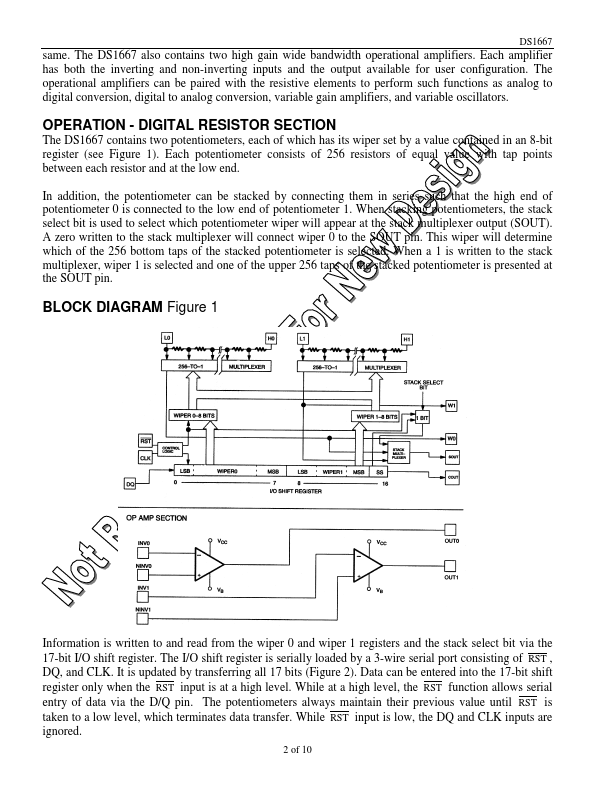
VCC GND L0, L1 H0, H1 W0, W1 VB SOUT
RST
DQ CLK COUT NINV0, NINVI INV0, INVI OUT0, OUT1
- +5-Volt Supply - Ground - Low End of Resistor - High End of Resistor - Wiper End of Resistor - Substrate Bias and OP AMP Negative Supply - Wiper for Stacked Configuration - Serial Port Reset Input - Serial Po
Key Features
Two digitally controlled 256-position potentiometers Serial port provides means for setting and reading both potentiometers Resistors can be connected in series to provide additional resolution Default wiper position on power up is 50% Resistive elements are temperaturecompensated to +20% end to end Two high-gain, wide bandwidth operational amplifiers Low power CMOS design.
Full PDF Text Transcription for DS1667 (Reference)
Note: Below is a high-fidelity text extraction (approx. 800 characters) for
DS1667. For precise diagrams, and layout, please refer to the original PDF.
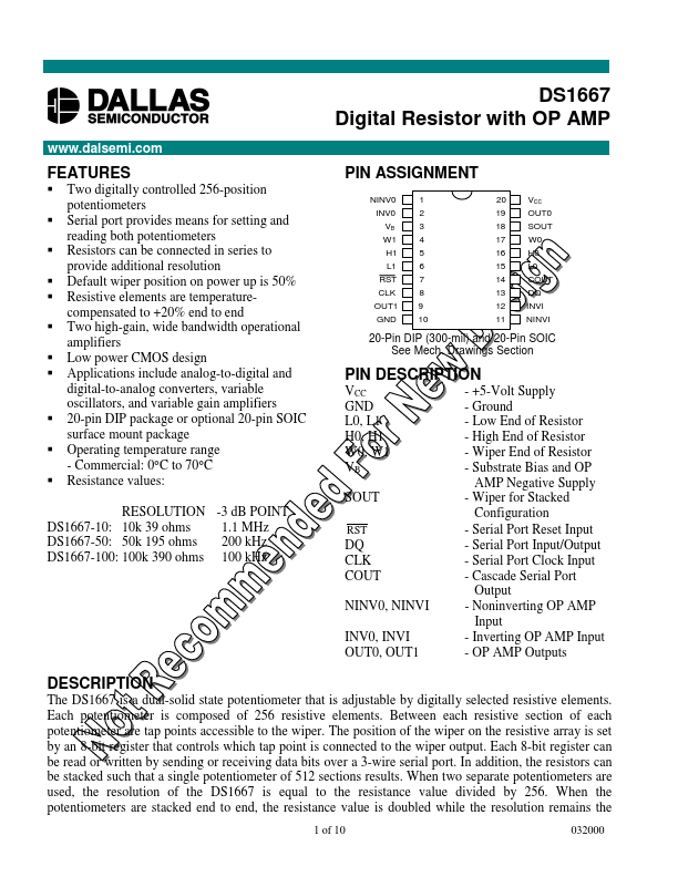
DS1667 Digital Resistor with OP AMP www.dalsemi.com FEATURES Two digitally controlled 256-position potentiometers Serial port provides means for setting and reading both ...
View more extracted text
otentiometers Serial port provides means for setting and reading both potentiometers Resistors can be connected in series to provide additional resolution Default wiper position on power up is 50% Resistive elements are temperaturecompensated to +20% end to end Two high-gain, wide bandwidth operational amplifiers Low power CMOS design Applications include analog-to-digital and digital-to-analog converters, variable oscillators, and variable gain amplifiers 20-pin DIP package or optional 20-pin SOIC surface mount package Operating temperature range - Commercial: 0°C to 70°C Resistance values: RESOLUTION -3 dB POINT DS1667-1
 DS1667 Datasheet