Click to expand full text
S6BP401A
Power Management IC for Automotive ADAS Platform
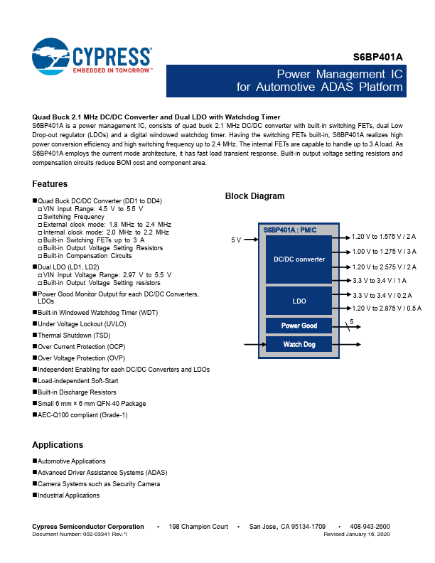
Quad Buck 2.1 MHz DC/DC Converter and Dual LDO with Watchdog Timer S6BP401A is a power management IC, consists of quad buck 2.1 MHz DC/DC converter with built-in switching FETs, dual Low Drop-out regulator (LDOs) and a digital windowed watchdog timer. Having the switching FETs built-in, S6BP401A realizes high power conversion efficiency and high switching frequency up to 2.4 MHz. The internal FETs are capable to handle up to 3 A load. As S6BP401A employs the current mode architecture, it has fast load transient response. Built-in output voltage setting resistors and compensation circuits reduce BOM cost and component area.
Features
◼Quad Buck DC/DC Converter (DD1 to DD4) VIN Input Range: 4.5 V to 5.
 S6BP401A Datasheet