Datasheet Details
| Part number | W232 |
|---|---|
| Manufacturer | Cypress (now Infineon) |
| File Size | 139.20 KB |
| Description | Ten Output Zero Delay Buffer |
| Datasheet |
 W232 Datasheet W232 Datasheet
|
|
|
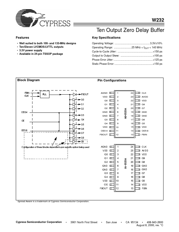
Reference Input: Output signals Q0:9 will be synchronized to this signal.
Feedback Input: This input must be fed by one of the outputs (typically FBOUT) to ensure proper functionality.
| Part number | W232 |
|---|---|
| Manufacturer | Cypress (now Infineon) |
| File Size | 139.20 KB |
| Description | Ten Output Zero Delay Buffer |
| Datasheet |
W232 Datasheet
|
|
|
|
| Part Number | Description |
|---|
The following content is an automatically extracted verbatim text from the original manufacturer datasheet and is provided for reference purposes only.