Datasheet4U Logo Datasheet4U.com

S70FL01GS - 1 Gbit (128 Mbyte) 3.0V SPI Flash

Datasheet Summary

Description

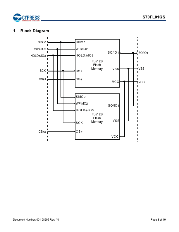
This document contains information for the S70FL01GS device, which is a dual die stack of two S25FL512S die.

For detailed specifications, refer to the discrete die datasheet provided in the Affected Documents/Related Documents table.

Features

  • CMOS 3.0V Core.
  • Serial Peripheral Interface (SPI) with Multi-I/O.
  • SPI Clock polarity and phase modes 0 and 3.
  • Double Data Rate (DDR) option.
  • Extended Addressing: 32-bit address.
  • Serial Command set and footprint compatible with S25FL-A, S25FL-K, and S25FL-P SPI families.
  • Multi I/O Command set and footprint compatible with S25FL-P SPI family.
  • READ Commands.
  • Normal, Fast, Dual, Quad, Fast DDR, Dual DDR, Quad DDR.
  • AutoBoo.

📥 Download Datasheet

Datasheet preview – S70FL01GS

Datasheet Details

Part number S70FL01GS
Manufacturer Cypress Semiconductor
File Size 422.92 KB
Description 1 Gbit (128 Mbyte) 3.0V SPI Flash
Datasheet download datasheet S70FL01GS Datasheet
Additional preview pages of the S70FL01GS datasheet.
Other Datasheets by Cypress Semiconductor

Full PDF Text Transcription

Click to expand full text
S70FL01GS 1 Gbit (128 Mbyte) 3.0V SPI Flash Features  CMOS 3.0V Core  Serial Peripheral Interface (SPI) with Multi-I/O – SPI Clock polarity and phase modes 0 and 3 – Double Data Rate (DDR) option – Extended Addressing: 32-bit address – Serial Command set and footprint compatible with S25FL-A, S25FL-K, and S25FL-P SPI families – Multi I/O Command set and footprint compatible with S25FL-P SPI family  READ Commands – Normal, Fast, Dual, Quad, Fast DDR, Dual DDR, Quad DDR – AutoBoot – power up or reset and execute a Normal or Quad read command automatically at a preselected address – Common Flash Interface (CFI) data for configuration information  Programming (1.5 Mbytes/s) – 512-byte Page Programming buffer – Quad-Input Page Programming (QPP) for slow clock systems  Erase (0.
Published: |