Datasheet4U Logo Datasheet4U.com

IMIC9531 - PCIX I/O System Clock Generator

Description

3] Pin[2] 3 4 1 14

24, 23, 22, 19, 18 8 XIN XOUT REF OE CLK(0:4) GOOD# Name PWR[4] VDDA VDDA VDD VDD VDDP VDD I/O I O O I O O Description Crystal Buffer Input Pin.

Connects to a crystal, or an external clock source.

Serves as input clock TCLK, in Test mode.

Features

  • Features.
  • Dedicated clock buffer power pins for reduced noise, crosstalk and jitter.
  • Input clock frequency of 25 MHz to 33 MHz.
  • Output frequencies of XINx1, XINx2, XINx3 and XINx4.
  • One output bank of 5 clocks.
  • One REF XIN clock output.
  • SMBus clock control interface for individual clock disabling and SSCG control.
  • Output clock duty cycle is 50% (± 5%).
  • < 250 ps skew between output clocks within a bank.
  • Output jitte.

📥 Download Datasheet

Full PDF Text Transcription

Click to expand full text
C9531 PCIX I/O System Clock Generator with EMI Control Features Features 
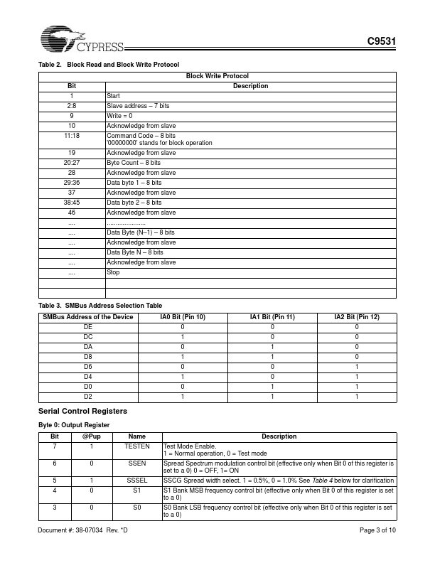
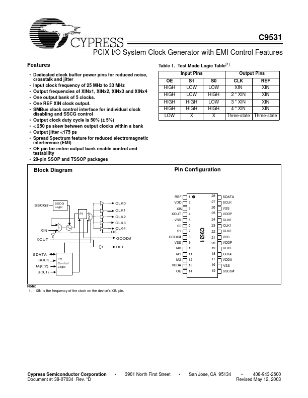
• Dedicated clock buffer power pins for reduced noise, crosstalk and jitter • Input clock frequency of 25 MHz to 33 MHz • Output frequencies of XINx1, XINx2, XINx3 and XINx4 • One output bank of 5 clocks. • One REF XIN clock output. • SMBus clock control interface for individual clock disabling and SSCG control • Output clock duty cycle is 50% (± 5%) • < 250 ps skew between output clocks within a bank • Output jitter <175 ps • Spread Spectrum feature for reduced electromagnetic interference (EMI) • OE pin for entire output bank enable control and testability • 28-pin SSOP and TSSOP packages Table 1.
Published: |