Datasheet Details
| Part number | CYWB0224ABS |
|---|---|
| Manufacturer | Cypress (Infineon) |
| File Size | 262.46 KB |
| Description | West Bridge Astoria |
| Datasheet |
 CYWB0224ABS Datasheet CYWB0224ABS Datasheet
|
|
|
Download the CYWB0224ABS datasheet PDF. This datasheet also covers the CYWB0224ABM variant, as both devices belong to the same west bridge astoria family and are provided as variant models within a single manufacturer datasheet.
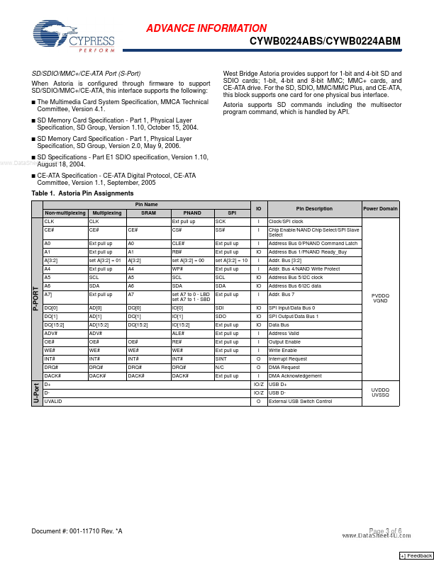
Clock/SPI clock Chip Enable/NAND Chip Select/SPI Slave Select Address Bus 0/PNAND Command Latch Address Bus 1/PNAND Ready_Buy Addr.
Bus [3:2] Addr.
Bus 4/NAND Write Protect Address Bus 5/I2C clock Address Bus 6/I2C data Addr.
| Part number | CYWB0224ABS |
|---|---|
| Manufacturer | Cypress (Infineon) |
| File Size | 262.46 KB |
| Description | West Bridge Astoria |
| Datasheet |
CYWB0224ABS Datasheet
|
|
|
|
| Part Number | Description | Manufacturer |
|---|---|---|
| CYW20706 | single-chip Bluetooth 5.4 LE SoC | INFINEON |
| CYW20707 | Bluetooth SoC | Cypress |
| CYW20719 | Bluetooth processor | Infineon |
| CYW20736 | Bluetooth Low Energy System-on-chip | Infineon |
| CYW20822-P4EPI040 | Bluetooth Low Energy module | Infineon |
| Part Number | Description |
|---|---|
| CYWB0224ABS | USB and Mass Storage Peripheral Controller |
| CYWB0224ABM | USB and Mass Storage Peripheral Controller |
| CYWB0224ABM | West Bridge Astoria |
| CYWB0220ABS | USB and Mass Storage Peripheral Controller |
| CYWB0226ABS | USB and Mass Storage Peripheral Controller |