Datasheet Details
| Part number | CY7C245A |
|---|---|
| Manufacturer | Cypress (Infineon) |
| File Size | 227.64 KB |
| Description | 2K x 8 Reprogrammable Registered PROM |
| Datasheet |
 CY7C245A Datasheet CY7C245A Datasheet
|
|
|
Download the CY7C245A datasheet PDF. This datasheet also covers the CY7 variant, as both devices belong to the same 2k x 8 reprogrammable registered prom family and are provided as variant models within a single manufacturer datasheet.
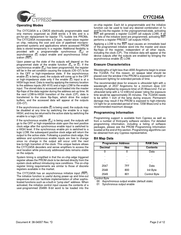
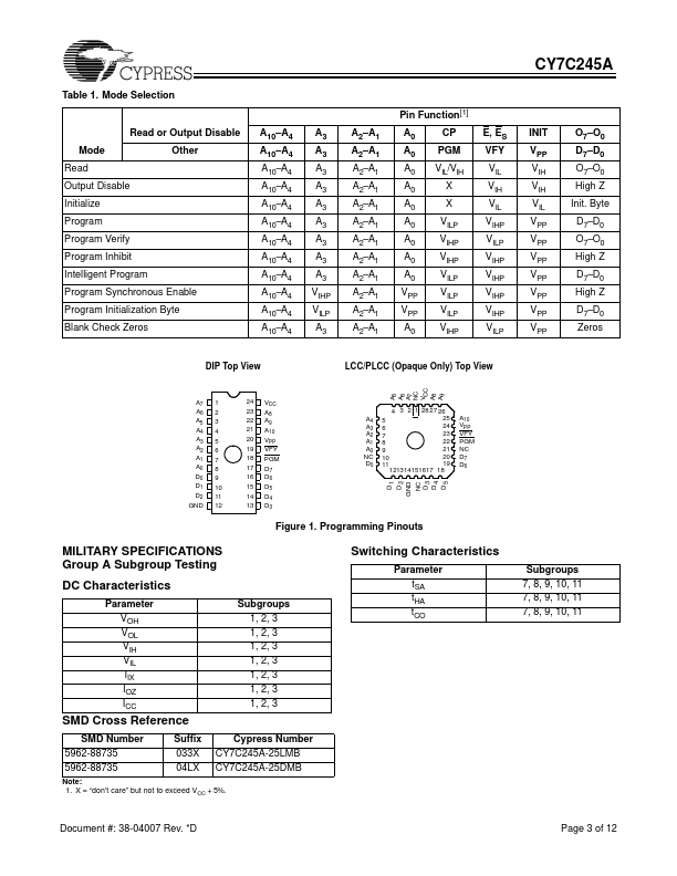
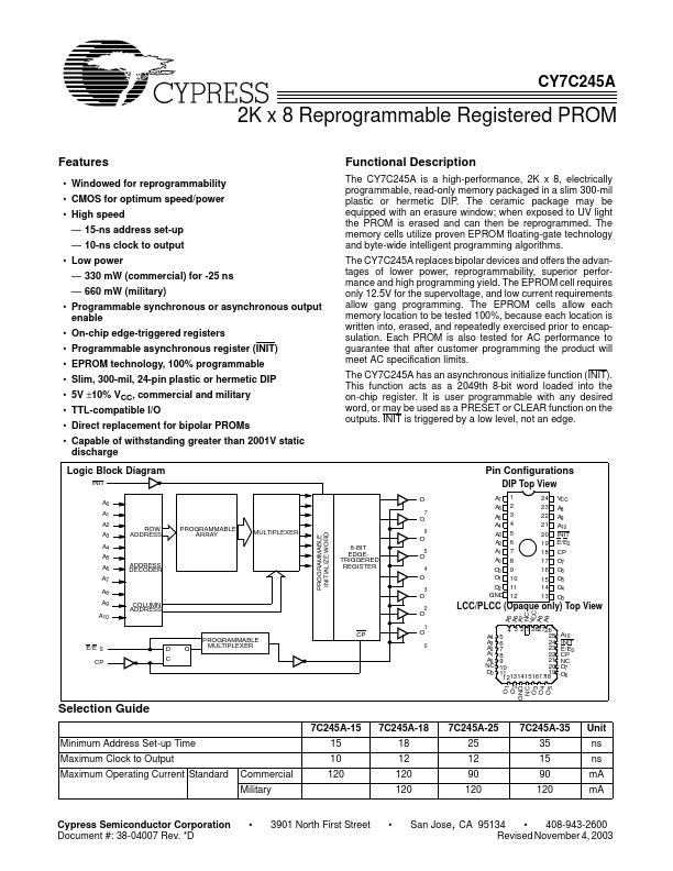
The CY7C245A is a high-performance, 2K x 8, electrically programmable, read-only memory packaged in a slim 300-mil plastic or hermetic DIP.
The ceramic package may be equipped with an erasure window; when exposed to UV light the PROM is erased and can then be reprogrammed.
| Part number | CY7C245A |
|---|---|
| Manufacturer | Cypress (Infineon) |
| File Size | 227.64 KB |
| Description | 2K x 8 Reprogrammable Registered PROM |
| Datasheet |
CY7C245A Datasheet
|
|
|
|
| Part Number | Description | Manufacturer |
|---|---|---|
| CY7C225 | 512 x 8 Registered PROM | Cypress |
| CY7C277 | 32K x 8 Reprogrammable Registered PROM | Cypress |
| CY7C008 | 64K/128K x 8/9 Dual-Port Static RAM | Cypress |
| CY7C008V | 3.3V 64K/128K x 8/9 Dual-Port Static RAM | Cypress |
| CY7C009 | 64K/128K x 8/9 Dual-Port Static RAM | Cypress |
| Part Number | Description |
|---|---|
| CY7C2163KV18 | 18-Mbit QDR II+ SRAM Four-Word Burst Architecture |
| CY7C2165KV18 | 18-Mbit QDR II+ SRAM Four-Word Burst Architecture |
| CY7C2168KV18 | 18-Mbit DDR II+ SRAM Two-Word Burst Architecture |
| CY7C2170KV18 | 18-Mbit DDR II+ SRAM Two-Word Burst Architecture |
| CY7C2245KV18 | 36-Mbit QDR II+ SRAM Four-Word Burst Architecture |
The following content is an automatically extracted verbatim text from the original manufacturer datasheet and is provided for reference purposes only.